Translate this page into:
The structural and optical properties of ZnO thin films prepared at different RF sputtering power
*Corresponding author. Tel.: +60 175272166; fax: +60 46579150 aia09_phy083@student.usm.my (A. Ismail)
-
Received: ,
Accepted: ,
This article was originally published by Elsevier and was migrated to Scientific Scholar after the change of Publisher.
Peer review under responsibility of King Saud University.

Available online 27 December 2012
Abstract
ZnO thin films were prepared on glass and Si(1 0 0) substrates by RF sputtering. The thickness, crystallinity, and the optical properties of the films were observed to vary with the RF power used. All the films exhibited preferred c-axis oriented (0 0 2) phase of wurtzite structure. The values of d-spacing for ZnO films were higher than those of the d-spacing for ZnO powder, suggesting that all the ZnO films experienced tensile strain. Good optical transmittance of 70–88% in the visible range has been observed in all the films. The PL spectra showed a dominant UV emission peak that shifted from 3.31 eV to 3.17 eV with decreasing RF power of the sample. The Raman lines around 433.26 cm−1 and 573.72 cm−1 attributed to E2 (high) and A1 (LO) respectively, were observed for all the ZnO films. The presence of tensile strain in the ZnO films was evident from the results of Raman spectra and XRD data. Defects due to oxygen vacancy in the prepared ZnO films were manifested in the PL and Raman spectra characteristics.
Keywords
Zinc oxide
Optical properties
X-ray diffraction
Photoluminescence and Raman spectra
1 Introduction
ZnO is well-known for various applications, such as varistors, gas sensors and transparent conductors for thin film transistors and solar cells. The other emerging applications include light emitting diodes (LEDs), laser diodes (LDs) and light detectors. These applications are attributed to the interesting material properties of a wide and direct band gap (3.37 eV) and high exciton binding energy (60 meV). The rich in defects is another important characteristic that has a direct impact on the electrical and optical properties of the material (Ozgur et al., 2005; Lau et al., 2005; Alivov et al., 2003; Chen et al., 2011; Singh et al., 2012; Sun et al., 2011; Qiao et al., 2012).
ZnO thin films can be prepared by techniques such as thermal oxidation (Rusu et al., 2007), chemical vapor deposition (Li et al., 2002), molecular beam epitaxy (Ohgaki et al., 2003) and pulsed laser deposition (Ryu and Zhu, 2000). The technique of RF sputtering has drawn considerable attention for ZnO film fabrication since the resulting film properties can be controlled by changing the sputtering conditions such as substrate temperature, deposition time, pressure, and RF power. However, the effect of changing the RF power on the ZnO film properties has not been much reported in the literature.
In this work, ZnO thin films were deposited by RF sputtering on Si(1 0 0) and glass substrates. The effect of the change in the RF power on the structural and optical properties of ZnO thin films was investigated.
2 Experimental
ZnO films were deposited by RF sputtering using high purity ZnO target of 7.6 cm diameter. The substrates used were n-type Si with (1 0 0) orientation and microscope slide glass. The substrates were initially cleaned with acetone and isopropanol in an ultrasonic bath for 15 min and rinsed with deionized water, before being fixed to a rotating substrate holder of the Edwards A500 RF sputtering unit at a distance of 10 cm above the ZnO target. Mechanical rotary pump and turbo pump were used to evacuate the sputtering chamber to its ultimate pressure of about 5 × 10⁻⁵ mbar. Argon (Ar) of high purity (99.99%) was used as sputtering gas. The pressure inside the chamber was maintained at 2 × 10⁻² mbar during the sputtering process. The ZnO films were deposited at different RF powers of 150 W, 175 W, 200 W, 225 W and 250 W for 50 min for each of the samples.
The optical properties of ZnO thin films were investigated by high-spatial resolution photoluminescence (PL), UV–visible spectrophotometer and Raman spectrometer. The Filmetrics F20 unit was used to determine the thickness of the prepared films. X-ray diffractometer (source Cu Kα with λ = 0.15406 nm) was used to characterize the structural properties of the ZnO thin films. The surface morphology of the film was determined using AFM and FESEM.
3 Results and discussion
Fig. 1 shows the increased thickness (t) of the prepared films with the increasing RF powers, indicating the proportionality of the number of atoms sputtered from the target to the applied RF power.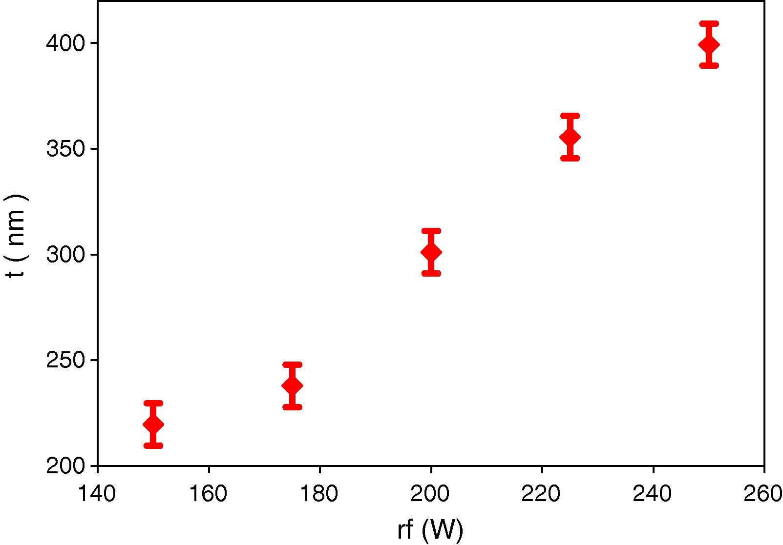
Thickness of the ZnO films on Si substrates as a function of the RF power.
Fig. 2 shows the XRD spectra for the prepared ZnO films from which the (0 0 2) peak of ZnO was observed for all the films. For films deposited at 200 W, 225 W and 250 W, (1 0 1) peak of ZnO was observed and its intensity increased with the increased RF power. However, for all the films the intensity of (0 0 2) peaks was higher as compared to the intensity of (1 0 1) peaks indicating that all the films were preferentially c-axis oriented. Furthermore, the (0 0 2) peaks were reduced for the RF power higher than 175 W indicating less favorable of (0 0 2) film orientation suggesting that the increase of RF power induced faster reaction rate that caused insufficient time for the formation of the initially preferred film orientation.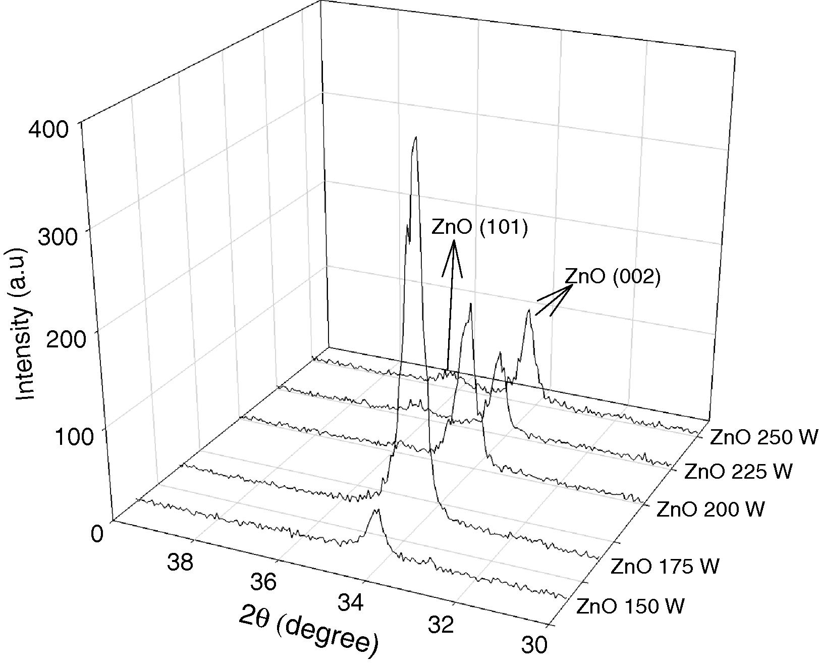
XRD spectra of ZnO films on Si substrates prepared at various RF powers.
The full width at half maximum (FWHM) of the diffraction peak can be used to estimate the crystallite size (D) in the grown films using Scherrer’s formula:
Sample
2θ (˚)
FWHM (˚)
d (Å)
c (Å)
strain (ɛ1)
D (nm)
ZnO 150 W
34.1865
0.246
2.6229
5.2458
0.749
35.3058
ZnO 175 W
34.1442
0.3936
2.6260
5.2521
0.869
22.0636
ZnO 200 W
34.1707
0.2460
2.6241
5.2481
0.794
35.3043
ZnO 225 W
34.1866
0.3444
2.6229
5.2458
0.749
25.2184
ZnO 250 W
34.2324
0.2952
2.6195
5.239
0.618
29.4251
Table 2 shows the increase of zinc (in %) with increasing RF power from 175 W to 250 W. While at the same time, the presence of oxygen (in %) tends to decrease. Thus, the O:Zn ratio in the film decreased with increasing RF power.
Sample
O K (at.%)
Zn L (at.%)
O/Zn ratio
ZnO 150 W
52.27
47.73
1.10 ± 0.18
ZnO 175 W
52.70
47.30
1.11 ± 0.2
ZnO 200 W
52.05
47.95
1.09 ± 0.2
ZnO 225 W
51.21
48.69
1.05 ± 0.2
ZnO 250 W
50.54
49.46
1.02 ± 0.2
The surface morphology of the films was characterized by AFM and FESEM (Fig. 3) which resulted in the root mean square (rms) of 2.01 nm, 2.81 nm, 7.25 nm, 12.20 nm and 14.83 nm for films prepared at RF powers of 150 W, 175 W, 200 W, 225 W and 250 W, respectively meaning that the root mean square (rms) increased with the increased thickness (t) of the prepared films. It was also observed that the shape of the grain changed from round to plate like as the RF power increased. The grain size changes randomly with increasing RF power, which agrees well with the XRD analysis.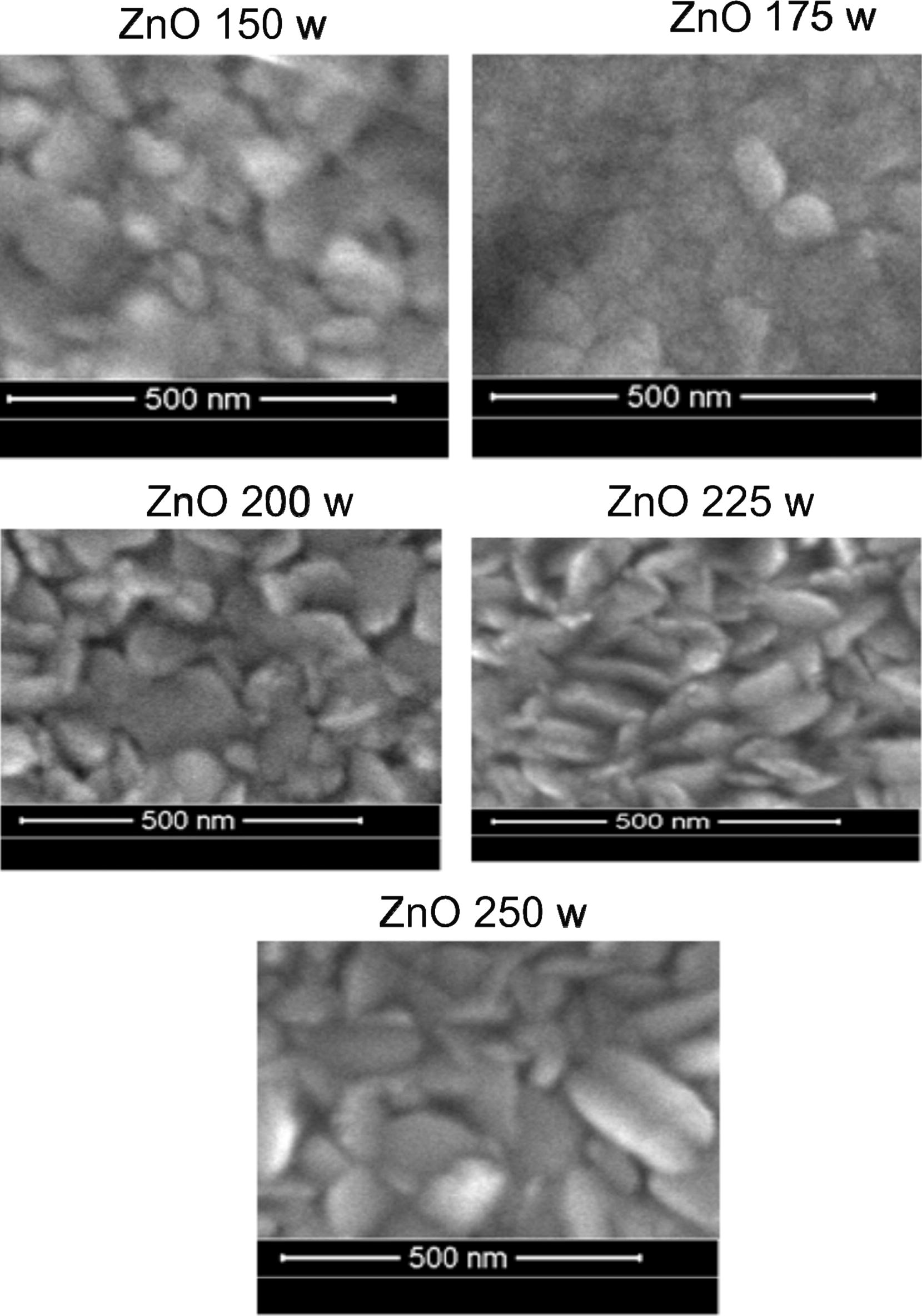
FESEM and AFM images of ZnO films on Si substrates prepared at various RF powers.
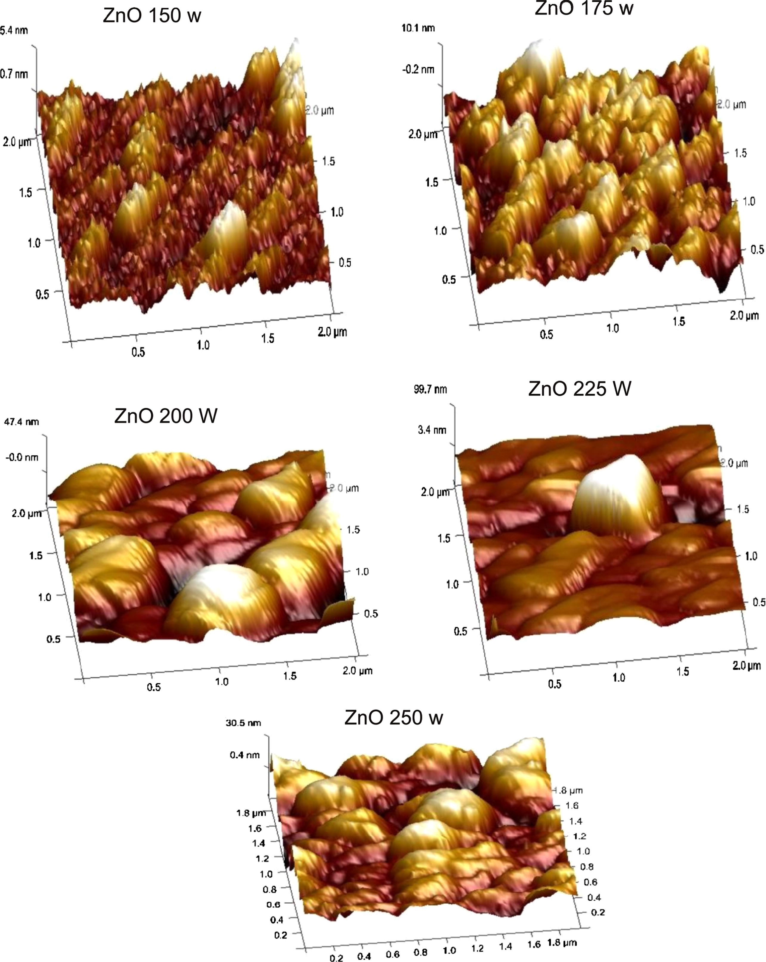
FESEM and AFM images of ZnO films on Si substrates prepared at various RF powers.
Fig. 4 shows the transmittance spectra of the ZnO films, which revealed a good optical transmittance of above 70% in the visible range (380–780 nm). The absorption coefficient (α) determined from the transmittance spectra is related to the photon energy (E) as given by:
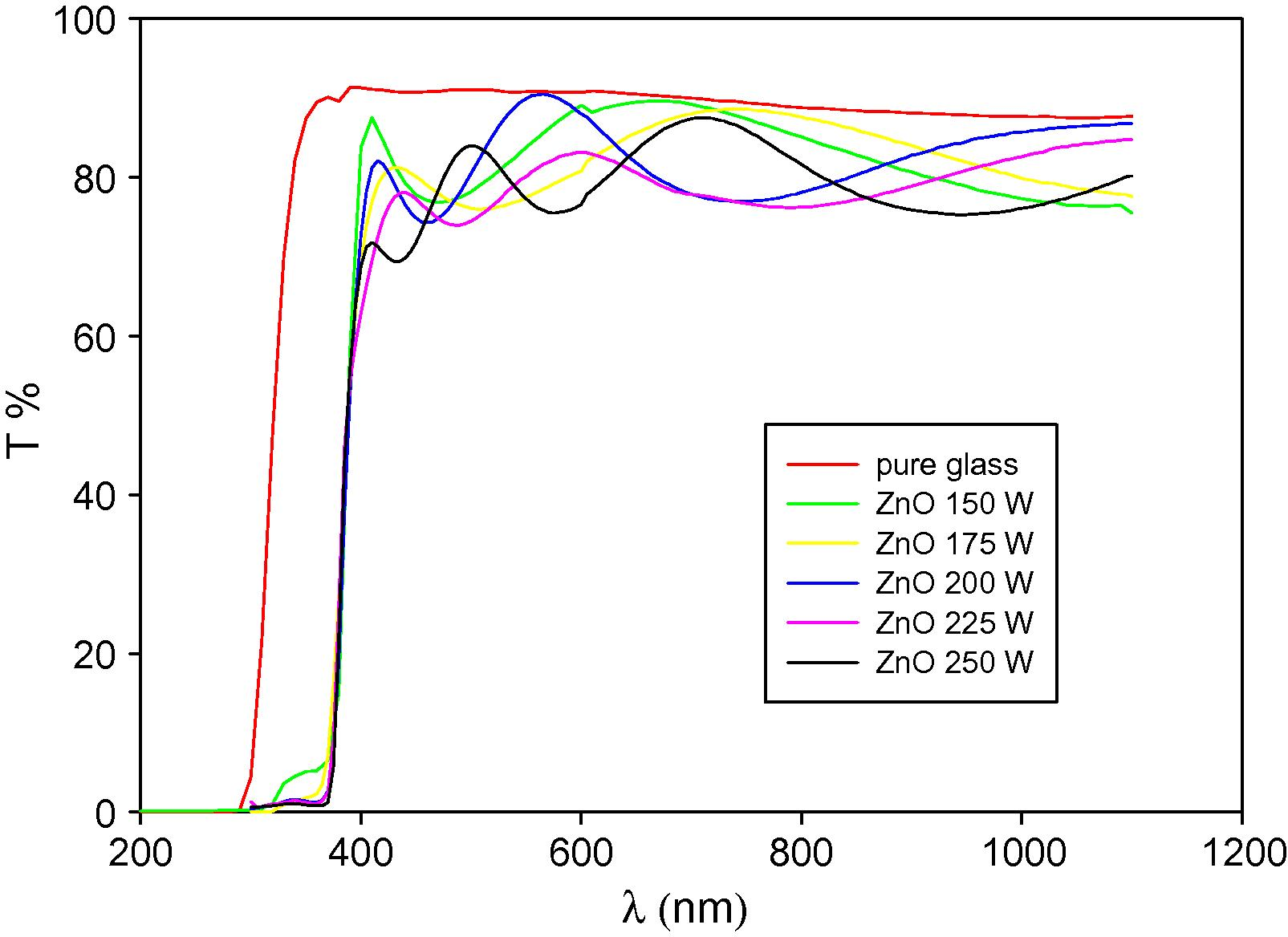
Transmittance spectra of the prepared ZnO thin films on glass substrates with different RF powers.
Fig. 5 shows the plot of (αE)2 versus E for the prepared samples which produced values of energy band gap of 3.29 eV, 3.26 eV, 3.25 eV, 3.23 eV and 3.24 eV for films prepared at RF powers of 150 W, 175 W, 200 W, 225 W and 250 W, respectively. Thus, the energy band gap was decreased with increasing RF powers with the values close to that of the published values of ZnO (Daniel et al., 2010; Al-Hardan et al., 2010) (Table 3 and Fig. 6).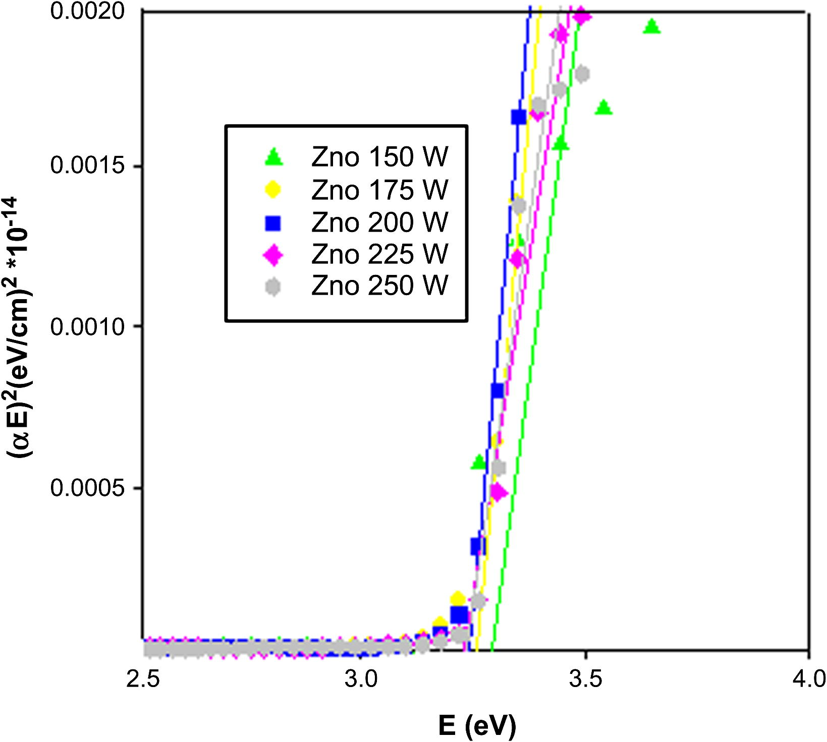
Photon energy (E) versus (αE)2 for ZnO thin films on glass substrates prepared at various RF powers.
Sample
Eg (eV)
Position of UV emission peak (eV)
ZnO 150 W
3.29
3.17
ZnO 175 W
3.26
3.26
ZnO 200 W
3.25
3.28
ZnO 225 W
3.23
3.27
ZnO 250 W
3.24
3.31
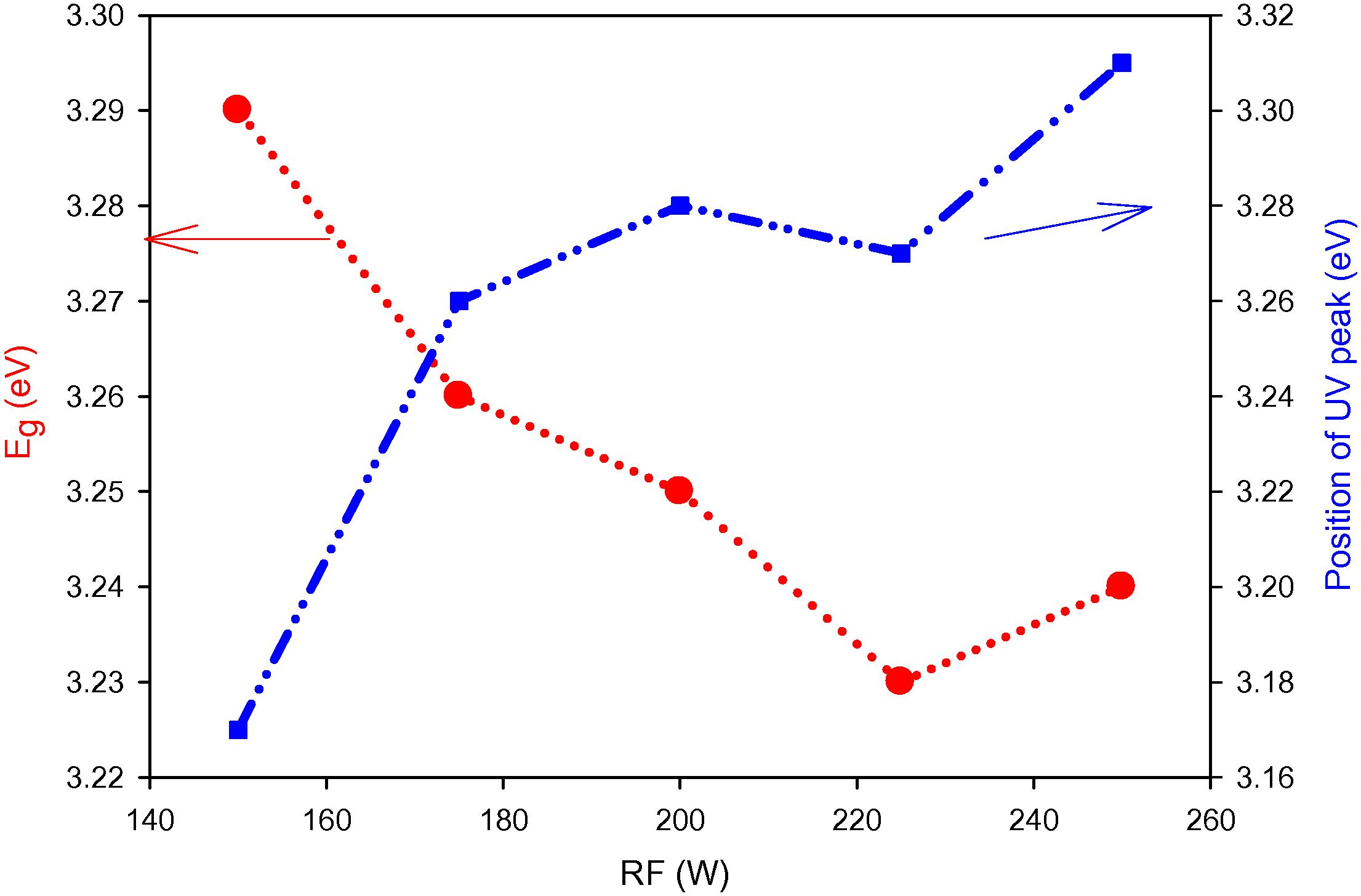
Energy band gap (Eg) and position of UV emission peak as a function of the RF power.
The refractive index n was calculated by the envelope method using the following equations (Al-Hardan et al., 2010).
Sample
Refractive index (n at 550 nm)
Refractive index (n at 600 nm)
Refractive index (n at 700 nm)
Refractive index (n at 800 nm)
ZnO 150 W
1.901
1.850
1.864
1.883
ZnO 175 W
1.964
1.891
1.856
1.856
ZnO 200 W
1.928
1.937
1.946
1.946
ZnO 225 W
2.009
1.991
1.973
1.991
ZnO 250 W
2.036
1.982
1.991
2.018
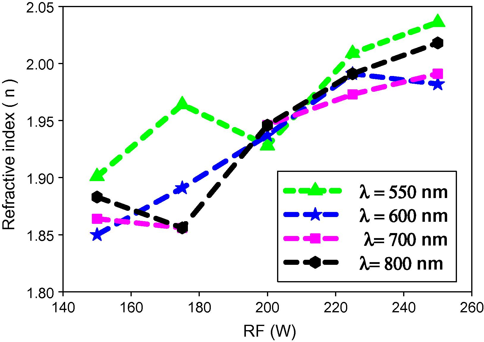
Refractive index n (at 550 nm, 600 nm, 700 nm and 800 nm) of ZnO films on Si substrates prepared at various RF powers.
The photoluminescence (PL) characteristics of the prepared ZnO thin films were obtained at room temperature in the photon energy range 1.24–4.1 eV. All the samples showed UV emission peaks as shown in Fig. 8(a). It was suggested that these peaks were attributed to the free excitons recombination and the strong UV emission in the PL spectra was an indication of a good crystalline structure of the film with excellent optical properties (Zhang et al., 2009). The observed UV emission appeared to be shifted toward higher energy (blue shift) with increasing RF power (Table 3 and Fig. 6). In addition, the observed weak green emission peak (2.36–2.46 eV) shown in Fig. 8(b) for ZnO (225 W) sample is ascribed to the oxygen vacancies (Lai and Lee, 2008).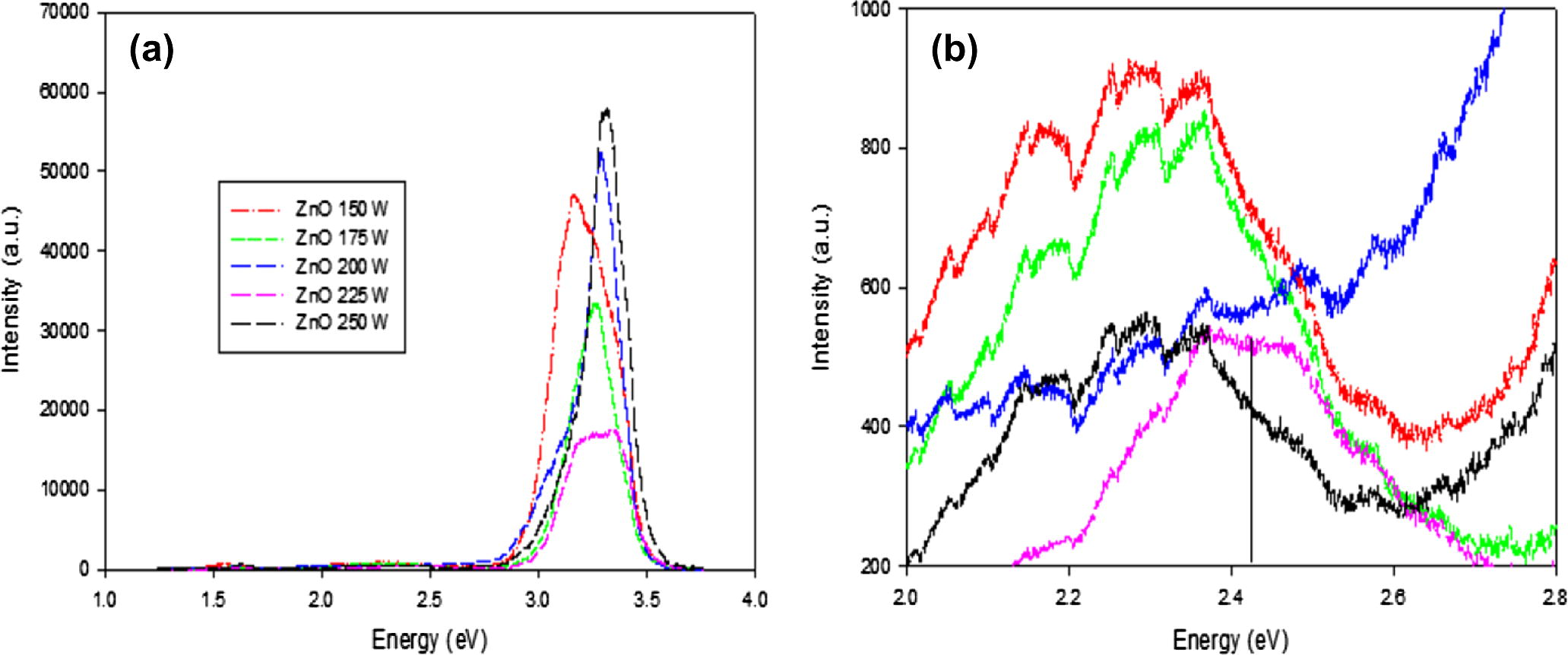
The effect of RF power on the PL spectra of ZnO thin films on Si substrates measured at room temperature.
Fig. 9 shows the Raman spectra of the prepared ZnO thin films where the Raman lines around 433.26 cm−1 and 573.72 cm−1 were observed for all the samples. These lines were assigned to ZnO E2 (high) and A1 longitudinal optical (LO) mode respectively (Cao and Du, 2007). The shift from 437 cm−1 to 433.26 cm−1 of E2 (high) was caused by the tensile strain in the films which was in good agreement with the XRD result (Ashkenov et al., 2003). The A1 (LO) mode was caused by the defects of O-vacancy and Zn interstitial. The increase of the A1 (LO) intensity for ZnO thin film prepared at RF (225 W) implied the increase of defects (O- vacancy and Zn interstitial) in this film which is consistent with the PL result of Fig. 8(b).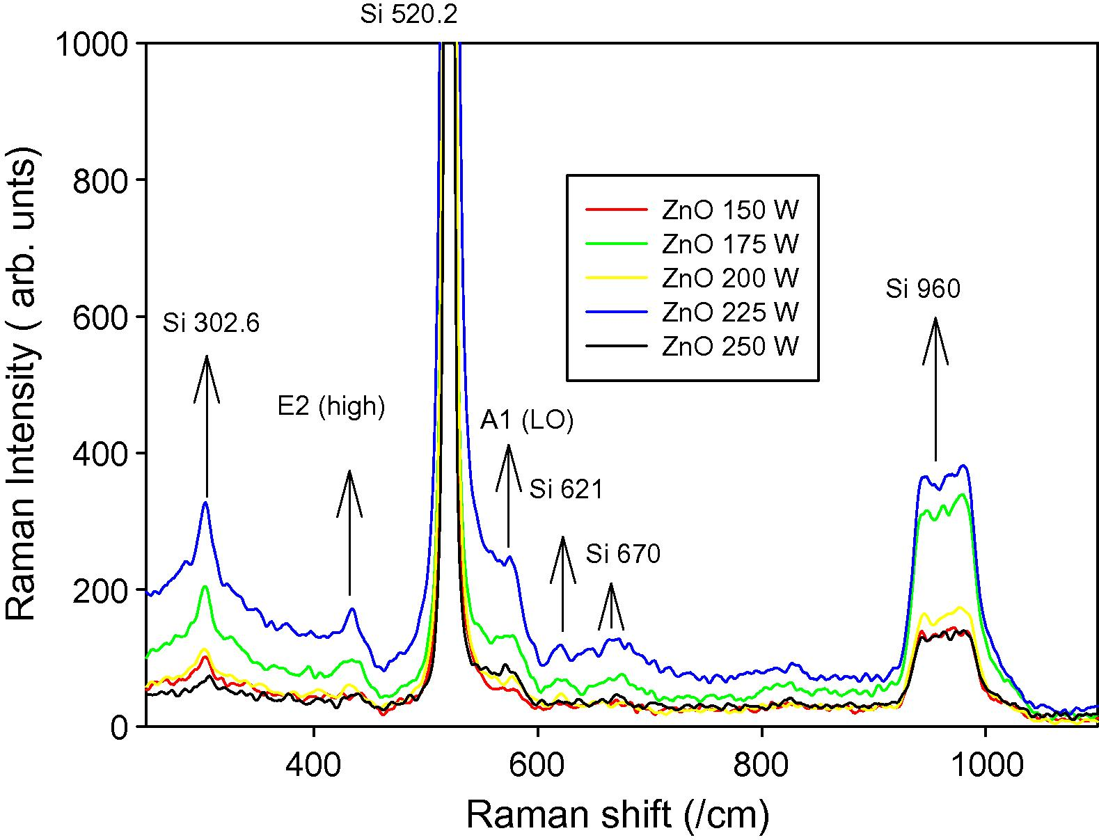
The effect of RF power on the Raman spectra of ZnO thin films on Si substrates measured at room temperature.
4 Conclusion
The effect of RF power on the structural and optical properties of sputtered ZnO thin films was investigated. XRD results revealed that all the ZnO films were dominantly grown in the c-axis orientation of wurtzite structure. The increase of the RF power (above 175 W) tends to reduce the tensile strain in the film. The observed UV emission peak revealed a blue shift with increasing RF power of the sample. The tensile strain in the films that caused the Raman lines shift was in good agreement with that obtained from the XRD result. The peak attributed to the oxygen vacancy defect in Raman spectra is consistent with that observed from PL spectra. The optical energy band gap decreased while the refractive index increased as the RF power of the sample increased.
Acknowledgements
This work was partly supported by a short term grant from the Universiti Sains Malaysia.
References
- The effect of oxygen ratio on the crystallography and optical emission properties of reactive RF sputtered ZnO films. Physica B. 2010;405(4):1081-1085.
- [Google Scholar]
- Fabrication and characterization of n-ZnO/p-AlGaN heterojunction light-emitting diodes on 6H-SiC substrates. Appl. Phys. Lett.. 2003;83(23):4719-4721.
- [Google Scholar]
- Infrared dielectric functions and phonon modes of high-quality ZnO films. J. Appl. Phys.. 2003;93(1):126.
- [Google Scholar]
- Strong exciton emission from ZnO microcrystal formed by continuous 532 nm laser irradiation. J. Lumin.. 2007;124(2):260-264.
- [Google Scholar]
- High-sensitivity NO2 gas sensors based on flower-like and tube-like ZnO nanomaterials. Sens. Actuators, B. 2011;157(2):565-574.
- [Google Scholar]
- Effect of annealing temperature on the structural and optical properties of ZnO thin films prepared by RF magnetron sputtering. Physica B. 2010;405(7):1782-1786.
- [Google Scholar]
- Influence of oxygen partial pressure on the structure and photoluminescence of direct current reactive magnetron sputtering ZnO thin films. Thin Solid Films. 2005;473(1):58-62.
- [Google Scholar]
- Investigation of optical and electrical properties of ZnO thin films. Mater. Chem. Phys.. 2008;110:393-396.
- [Google Scholar]
- Laser action in ZnO nanoneedles selectively grown on silicon and plastic substrates. Appl. Phys. Lett.. 2005;87(1):013104.
- [Google Scholar]
- High quality ZnO thin films grown by plasma enhanced chemical vapor deposition. J. Appl. Phys.. 2002;91(1):501.
- [Google Scholar]
- Growth condition dependence of morphology and electric properties of ZnO films on sapphire substrates prepared by molecular beam epitaxy. J. Appl. Phys.. 2003;93(4):1961.
- [Google Scholar]
- A comprehensive review of ZnO materials and devices. J. Appl. Phys.. 2005;98(4) 041301-103
- [Google Scholar]
- Light-emitting diodes fabricated from small-size ZnO quantum dots. Mater. Lett.. 2012;74:104-106.
- [Google Scholar]
- Preparation and characterization of ZnO thin films prepared by thermal oxidation of evaporated Zn thin films. Superlattices Microstruct.. 2007;42(1–6):116-122.
- [Google Scholar]
- Optical and structural properties of ZnO films deposited on GaAs by pulsed laser deposition. J. Appl. Phys.. 2000;88(1):201.
- [Google Scholar]
- Pulse-like highly selective gas sensors based on ZnO nanostructures synthesized by a chemical route: effect of in doping and Pd loading. Sens. Actuators, B. 2012;166–167:678-684.
- [Google Scholar]
- Ultraviolet electroluminescence from ZnO-based light-emitting diode with p-ZnO:N/n-GaN:Si heterojunction structure. J. Lumin.. 2011;131(4):825-828.
- [Google Scholar]
- Photoluminescence and Raman scattering of ZnO nanorods. Solid State Sci.. 2009;11(4):865-869.
- [Google Scholar]


