

Translate this page into:
Synthesis of nanocomposite films based on conjugated oligomer-2D layered MoS2 as potential candidate for optoelectronic devices
⁎Corresponding author at: Department of Physics and Astronomy, College of Science, King Saud University, P.O. Box. 2455, Riyadh, Saudi Arabia. malsalhi@ksu.edu.sa (Mohamad S. AlSalhi)
-
Received: ,
Accepted: ,
This article was originally published by Elsevier and was migrated to Scientific Scholar after the change of Publisher.
Peer review under responsibility of King Saud University.
Abstract
In this investigation, we have analyzed the structural, electrical, and optical behaviors of pure and composite thin films which are obtained from 2D monolayer molybdenum disulfide (MoS2) flakes, conjugated oligomer (CO) 1,4-Bis(9-ethyl-3-carbazo-vinylene)-9,9-dihexyl-fluorene (BECV-DHF), and by combining CO (BECV-DHF) with MoS2 in forms of CO/MoS2 composites. All the samples are coated on SiO2/Si substrates using the spin coating procedure where a spin-coating solution has been obtained by dispersing CO and MoS2 in ethanol or toluene. The structural morphology of MoS2 films and CO/MoS2 films of various thicknesses are analyzed using field emission scanning electron microscope (FE-SEM), transmission electron microscope (TEM), and profilometer. These experimental results confirm the formation of MoS2 layer composite with oligomer nanocrystals. The optical properties of MoS2, CO, and CO/MoS2 films showed that the increased film thickness shifted the spectral peaks towards near infrared (NIR) and ultraviolet–visible (UV) regions of the electromagnetic spectrum. Moreover, devices such as solar cells, flexible memory cell and MOSFET were designed. The I-V characteristics of these devices show that CO/MoS2 composite films could serve as potential candidates for organic-inorganic nano-electronic device applications.
Keywords
Thin films
Molybdenum disulfide
Conjugated oligomer
Optical properties
Nanoelectronic devices

1 Introduction
Owing to its impressive physico-chemical features, the two-dimensional (2D) honeycomb graphene lattice has captivated a considerable interest in the materials research community (Lee et al., 2008). Since the experimental synthesis of graphene, numerous 2D materials have actively been established, which disclose fascinating physical properties. This can partially be attributed to the fact that the application of graphene in electronic and optoelectronic devices is strained due to its semimetallic behavior (with zero bandgaps) under normal conditions. However, inorganic materials such as transition metal dichalcogenides (TMDs) are now available in 2D forms, which are structurally analogous to graphene but show significantly different physical properties suitable for semiconductor technologies (Lee et al., 2008, Duan et al., 2015, Eda et al., 2011). In particular, the 2D layered modification of MoS2 has aroused prominent attention for its applications in several technological applications such as energy storage devices, field-effect transistors (FETs) devices, chemical sensors, photodetectors, photovoltaics, and solar cells (Cao et al., 2016, Shanmugam et al., 2012, Xu et al., 2014). In its bulk form, MoS2 possesses a crystal structure similar to graphite, which is an ideal structure whereby 2D layers are joined together via weak van der Waals interactions (Duan et al., 2015). Consequently, exfoliation of MoS2 can easily be realized for obtaining nano-layers instead of resorting to other complicated techniques for synthesizing 2D materials (Duan et al., 2015).
Since the discovery of organic molecular and polymeric semiconductors, a diversity of semiconducting systems have been identified, which are commonly termed as conjugated materials and constitute a fascinating class of materials for applications in photonic devices (Riaz et al., 2016; Stejskal, 2015; Jadoun et al., 2017; Riaz et al, 2017). A huge research interest focused on these conjugated materials stems from their potentials functionalities, which are suited to optoelectronic devices such as light-emitting diodes, organic field-effect transistors (OFETs), and laser optical media, etc. (Riaz et al, 2017; Collins et al., 2017). From among the conjugated materials, a conjugated oligomer (CO) consists of a light molecular weight combined with a distinctive molecular structure which exhibits replication of a small number of units as well as an ordered repetitive structure (mono-dispersive and regio-regularity) (Aljaafreh et al., 2019; AlSalhi et al., 2020, 2018; Abdulaziz Alfahd et al., 2017; Anni, 2019; Milad et al., 2016; Alwan et al., 2017; Ma and Shi, 2013). Conjugated oligomers (COs) such as 1,4-Bis(9-ethyl-3-carbazo-vinylene)-9,9-dihexyl-fluorene (BECV-DHF) represent potential candidates with exceptional properties when compared with the conjugated polymers due to the controllable length of the conjugate and the ability to limit separation of the number of units (AlSalhi et al., 2018). Accordingly, their accessibility of preparation is feasible, and their deposition as a thin film can easily be attained via low-cost synthesis techniques such as spin coating (Milad et al., 2016; Yang et al., 2017). In addition, superior compatibility of the COs with inorganic materials has also made them attractive for blended, composite, and hybrid systems (Ma and Shi, 2013).
From the above discussion, it can be inferred that combining 2D-TMDs with COs in the form of thin films may provide novel composite material for optoelectronic device applications. In fact, MoS2 has already been used in obtaining novel nanocomposites, biomaterials, and transistors (Anbazhagan et al., 2016; Feng et al., 2016; Paul and Robeson, 2008; Zachariah et al., 2014; Tanaka et al, 2015; Chu et al., 2016; Zhang et al., 2013). In particular, investigations on the integration of other COs with 2D layered material such as MoS2 have previously been reported (Ma and Shi, 2013; Jariwala et al., 2016; Friedman et al., 2016; Chen et al., 2016; Shastry et al., 2016), which show that organic/inorganic thin films constitute p-n junction behavior that could even be beneficial for photovoltaic (Chen et al., 2016, Shastry et al., 2016,), motivated by these reasons, in the present study we have synthesized and characterized CO/MoS2 films to obtain a clear understanding regarding the electrical and optical properties of composites between BECV-DHF and 2D MoS2.
We aim to simultaneously inspect and compare the structural morphology, film profile, chemical composition, optical properties, and I-V characteristics of spin-coated MoS2 and CO/MoS2 thin films. We anticipate that the CO/MoS2 thin films studied in the present work could procure applications in optoelectronic devices.
2 Materials and methods
For this work, molybdenum disulfide nanoflakes (nf-MoS2), ITO substrates, and poly(3,4-ethylenedioxythiophene) polystyrene sulfonate (PEDOT:PSS) have been purchased from Ossila, UK. While 90-nm thick SiO2/Si substrates purchased from Nanografi Nano Technology, Ankara, Turkey. The oligomer used in this work is called the 1,4-Bis(9-ethyl-3-carbazo-vinylene)-9,9-dihexyl-fluorene (BECV-DHF), which has a molecular weight of about 773.12 g mol−1 (the molecular structure is displayed in Fig. 1, as described in Ref. (Abdulaziz Alfahd et al., 2017). Polyethylene terephthalate (PET) sheets, aluminium oxide (Al2O3), ethanol, acetone, and toluene provided by Sigma Aldrich, St. Louis, MO, United States are used. Reduced graphene oxide: multiwalled carbon nanotubes (rGO:mCNT) based conductive ink is purchased from Ad-Nano Technologies, Shivamogga, Karnataka, India.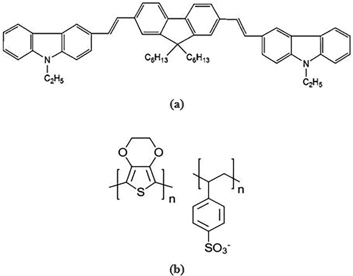
The structural model of molecule of (a) conductive oligomer 1,4-Bis(9-ethyl-3-carbazo-vinylene)-9,9-dihexyl-fluorene (BECV-DHF) [17) and (b) conjugated-polymer Poly(3,4-ethylenedioxythiophene) polystyrene sulfonate.
2.1 The preparation CO/MoS2 composite
Following the procedure modified method of Ref. (Yang et al. 2017), we have prepared a MoS2 solution for use in the spin coating procedure. For a comparison between various properties, we prepared samples soluble in two different solvents, such as toluene and ethanol. A sufficient quantity (40 ml) of as-received solution (DI: Methanol: MoS2) was dropped into a beaker and heated to 80 °C for 10 min. Few drops of acetone are added to the solution to reduce the boiling point of the MoS2 containing solution. The vapors were gently removed by a mounted exhaust fan. Immediately after all liquid evaporated, the beaker was removed from the heater and cool to room temperature. The required solvent (ethanol or toluene) was added and sonicated to disperse the MoS2 into the new solvent. The resulting solution was topped up with solvent to maintain 20 mg/ 1 ml. Next, the oligomer was dissolved into the required solution (ethanol or toluene) to form a concentration of 20 mg/1 ml and sonication. Finally, the oligomer and MoS2 solutions were added in a 1:1 ratio to form the final solution. Here, 1 ml of MoS2 solution is added to 1 ml of oligomer. The resulting solution contained 10 mg/ ml of MoS2 and oligomer. The final solution was translucent blackish-blue in color, as shown in Fig. 2 (a).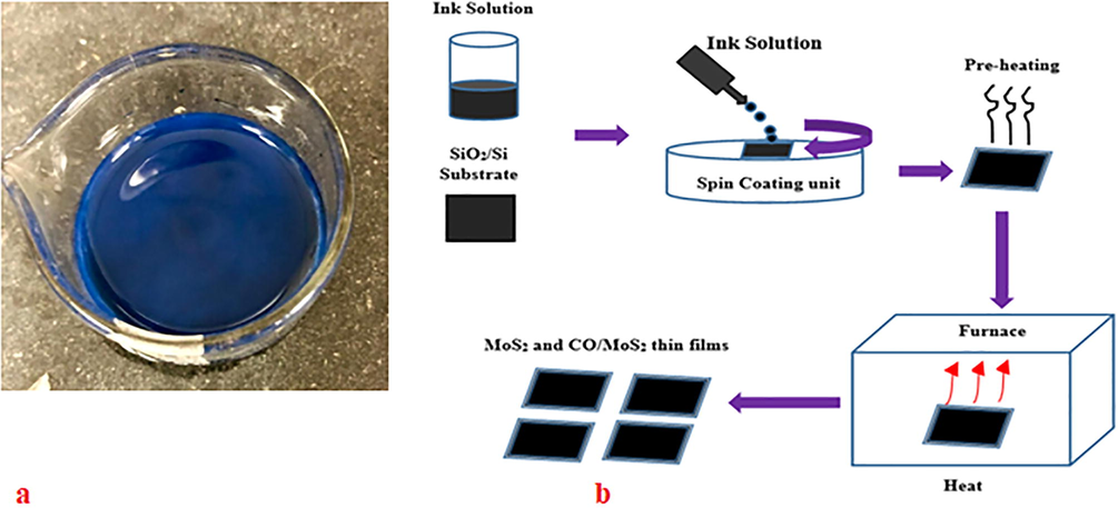
(a) CO/MoS2 blend in toluene (b). Procedure of spin coating for preparing MoS2 and CO/MoS2 thin film.
Other samples were dispersed in toluene and coated by spin-coating technique at various speeds for 30 sec to compare them with the above-prepared films. The CO (BECV-DHF) solution was obtained with the dissolution of 1 mg of oligomer in 1 ml of toluene or ethanol (1:1 v/v) solution. The spin coating of the solution is dropped on SiO2/Si substrate and deposited at varying speeds (1000–4000) r.p.m. for 30 sec. The composite solution was prepared using equal amounts of pure MoS2 and oligomer solution. Before the spin coating of the final solution, it was ink sonicated for 5 min. The spin-coating of the ink solution was performed three times for all samples on the 90-nm-thick SiO2/Si substrate at different speeds from 500 to 4000 r.p.m. for 30 s (see Fig. 2 (b)). The different speed method is adopted to study the changes in photo physical and photo-electrical properties induced due to different thickness and morphology, which imported due to coating at different spin speed.
2.2 The device fabrication procedure
Memory cell is designed using polyethylene terephthalate (PET) as substrate. A layer of rGO:mCNT is coated using spin coating at 2000 rpm. Next, five layers of CO:MoS2 (1:1) was dropped at 3000 rpm. Finally, a layer of Al of 150 nm thickness is deposited using vacuum thermal deposition method. The structure of memory device is PET/rGO:mCNT/BECV-DHF:MoS2/Al.
Solar cells are made by spin coating a 30 nm layer of PEDOT:PSS on ozone treated ITO substrate. Next layer contained one of the MoS2, CO, or CO:MoS2 spin coated at 2000 rpm. Finally layers of calcium and aluminum were coated using vacuum thermal evaporation method. The configuration of designed solar cells are varied as follows, (a) ITO/MoS2/Ca/Al, (b) ITO/BECV-DHF/Ca/Al, (c) ITO/PEDOT:PSS/MoS2/Ca/Al, (d) ITO/PEDOT:PSS/BECV-DHF:MoS2 (1000 rpm)/Ca/Al, (e) ITO/PEDOT:PSS/BECV-DHF:MoS2 (2000 rpm)/Ca/Al, and (f) ITO/PEDOT:PSS/BECV-DHF:MoS2/Ca/Al.
2.3 Characterization and measurement techniques
After preparing the solution of MoS2, the morphological structures of small particles (magnitude between nm and µm) are examined with the aid of the transmission electron microscopy (TEM) having model JEM-1400 plus manufactured by JEOL, Japan. The XRD patterns of MoS2, CO, and CO/MoS2 synthesized samples are established by employing a D8 Advance Bruker diffractometer, with a Cu-Kα radiation source of the wavelength of 0.1542 nm. The morphological structural are characterized with the support of JSM-7610F FE-SEM produced by JEOL. The measurements of the film’s thicknesses are determined with the profilometer. The Fourier transform infrared (FTIR, Nicolet 6700, Thermo Scientific, USA) spectra are measured for CO/MoS2 films to analyze; the structural bonding, the transmission modes, and the wavenumber regime are selected between 350 and 4000 cm−1. The recording of the optical absorbance spectra of the CO/MoS2 films was carried out with the assistance of JASCO UV/VIS/NIR spectrophotometer (V-770), and the wavelength regime was spanned between 200 and 1200 nm. This could reveal the exciting applications of MoS2 film in optoelectronics, night-vision imaging, or photovoltaics. By employing monochromatized Al Kα at 1486.6 eV, the measurements of the binding energies of the elements involved in the films are accomplished with the aid of XPS spectra, namely PHI 5600 Multi-Technique XPS (XPS, Physical Electronics, Lake Drive East, Chanhassen, MN, USA). The fitting of peaks is carried out with the assistance of CASA XPS Version 2.3.14 software. I-V characterization of memory device and solar cells were measured using opti-scense (FYTRONICS) solar simulator from USA.
3 Results and discussion
3.1 Surface morphology and X-ray diffraction patterns:
The FE-SEM topography was carried out to measures changes in the morphological pattern of CO/MoS2 composites where the films are dispersed homogeneously (see Fig. 3. a). The coating of Platinum was done on CO/MoS2 films for 40 sec before performing SEM. It is well noticed that the MoS2 nanoflakes are few layers stacked. Few of them are project outward; on top of the MoS2 flakes, the oligomers crystals were present in different shapes and sizes. The oligomers crystals have very thin ridge gapes, which is about 2 nm wide. These nanoridges could improve the photoelectric properties of the blend through plasmonic generation.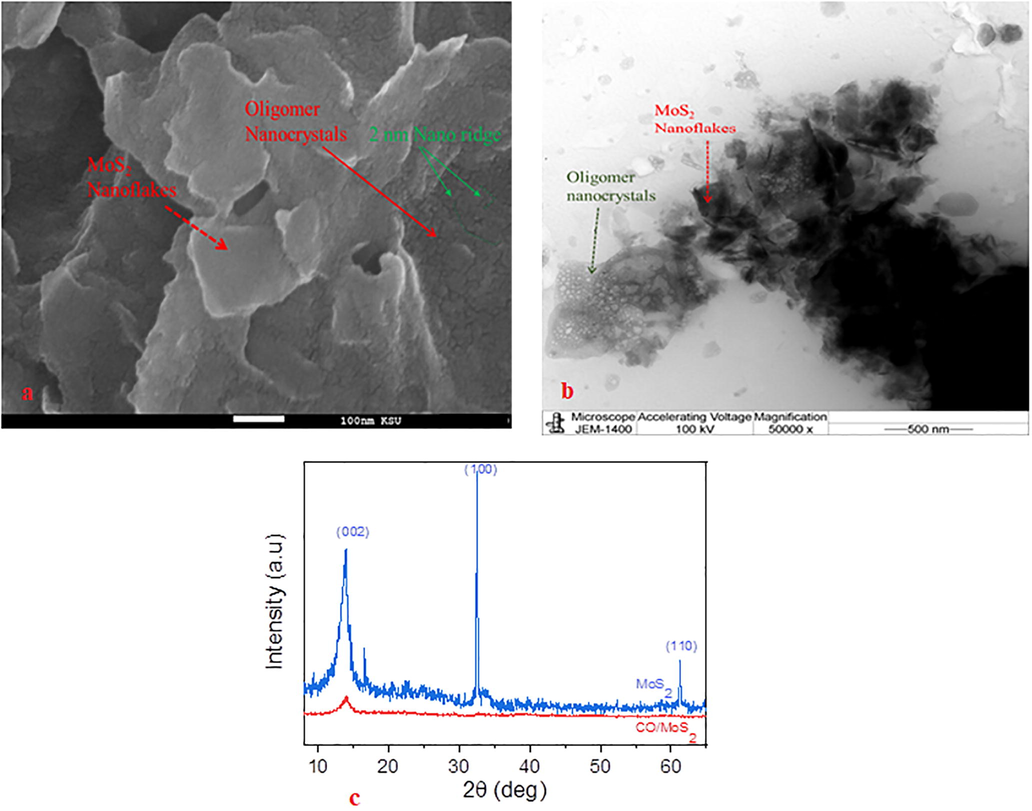
(a) FE-SEM images of the composite CO/MoS2, (b) HR-TEM images of the composite CO/MoS2 and (c) x-ray diffraction diagrams of both pure MoS2 films and CO/MoS2 samples.
The HR-TEM image in Fig. 3 (b) shows the formation of oligomer nanocrystals formed on top of MoS2 flakes. The average grain size of crystals is around 50 nm. The SEM and TEM analysis show the formation of CO/MoS2 composite. The strong adherence of oligomer on MoS2 would improve the physical properties and also enable ease of device fabrication using this composite material.
The XRD patterns of MoS2 films and CO/MoS2 composites are displayed in Fig. 3c. Many marked sharp and small peaks for MoS2 films are observed at 14.1°, 32.8°, and 59.1°, respectively, that are related to the (0 0 2), (1 0 0), and (1 1 0) crystallographic planes (Zeng et al., 2013). As clearly seen from Fig. 3c, the XRD patterns of pure MoS2 films and CO/MoS2 exhibit quite similar features in the range of 2θ = 10°–25°. The first feature peak in both pure MoS2 and CO/MoS2 composites represent the most important peak since the remaining diffracted planes occurring with weak diffracted and insignificant intensities for CO/MoS2 composites. It is well noticed for CO/MoS2 composites that the XRD pattern preserves the crystal structure of MoS2 flakes. A pronounced sharper peak occurs at 13.9° that corresponds to the (0 0 2) plane, which is only the characteristic peak of MoS2 films. The feature peak of CO/MoS2 is displaced to the relatively marginal position of angle of 2θ = 13.95°, which surmises the intercalation of CO into MoS2 flakes. This implies the appearance of MoS2 in composites (Aljaafreh et al., 2019; Tanaka et al., 2015). It is inferred that the composites acquire quite analogous physical properties to those of MoS2 flakes.
3.2 XPS analysis
The bonding guidance and compositional elements in MoS2 films, CO, and CO/MoS2 composites are inspected from XPS. The survey scan of the high-resolution pattern of these elements are illustrated in Fig. 4. It is shown that the XPS survey spectrum records the compositional elements of Mo, S, C, O, and N at specific regions. The core-level spectrum of C1s illustrates a peak located around 284.1 eV that is related to the C-N bond. Note that this weak peak is associated with p–p interaction, leading to the interaction between CO and MoS2. The N1s XPS spectrum displays a peak at 399.75 eV. The Mo 3d curve exhibits peaks at 232.8 eV, while the S 2p small peaks occur around 169.1 eV that can be split into doublet Sp1/2 and Sp3/2, respectively.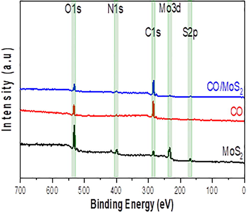
The survey scan of compositional elements in MoS2 films, CO, and CO/MoS2 composites.
As clearly apparent from Fig. 5, all spectra of molybdenum 3d element of MoS2 and CO/MoS2 dissolved in ethanol and toluene show almost indistinguishable peaks associated with Mo that are bonded to the S atoms. The main contribution of Mo peaks comes from MoS2 along with an insignificant contribution of the ethanol or toluene precursors. The spectral region of the pure MoS2 films depicted in Fig. 5(a-b) contains the fitting of the three characteristics which can be attributed to the Mo-3d core state signals. A significantly intense peak, centered at a binding energy of 232.3 eV, is associated with Mo-3d3/2 of Mo atoms in the vicinity of S atoms. The spectral peak of pure MoS2 positioned about 227.3 eV of binding energy originates through the defect of Mo-3d5/2 in MoS2. Also, the peaks laying at binding energies around 235.5 and 232.2 eV are due to Mo6+ of the unreacted precursor solvents, which is always found as a contaminant on MoS2 film synthesized via spin coating. It is evident from Fig. 5 that the usual peaks linked to Mo and S elements in MoS2 are not significantly changed after their hybridization with CO. This can be ascribed to Mo’s weak assistance to the surface reactions and van der Waals interactions between the polymer and MoS2 films. Hence, in Fig. 5, an additional peak emerges at a binding energy of 227.1 eV, which is linked to a sulfur atom near a defect site. Moreover, the most intense peak is essentially due to Mo-3d5/2.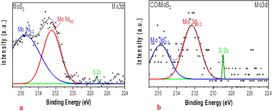
XPS spectra of Mo-3d core-level regions of (a) MoS2 and (b) CO/MoS2.
3.3 Fourier transform infrared (FTIR) investigation
The FTIR spectra display in Fig. 6, the MoS2 and CO/MoS2 films soluble in both ethanol and toluene solvents. These are assigned to vibrational modes in groups of MoS2 and other elements arising from CO and solvents that are involved in the reaction system. Fig. 6 displays the occurrence of a marked peak about 1098 cm−1 corresponding to the physisorption of ethanol precursor. FTIR spectra of MoS2 and CO/MoS2 dissolved in toluene thin films display broad peaks at about 3450 and 2350 cm−1 of C–H and S-H bond, respectively. However, these peaks occur for MoS2 and CO/MoS2 dissolved in ethanol. FTIR spectrum exhibits a sharp peak roughly about 1600 cm−1 and 1450 cm−1 because the C–C bond are stretched (νcc) (Syariati et al., 2019) as well as the bending of the O-C bond. A strong peak is observed in all samples at 705 and 473 cm−1 revealing C-S (νcs) (Choi et al., 2012) and Si-O stretching vibration, respectively. These results are in agreement with the XPS spectra presented earlier and demonstrated that the addition of the CO can effectively alter the surface of MoS2. The spectral peak located around 531 cm−1 is owing to the stretching of the S-Mo-S bond. FTIR spectra of CO/MoS2 dissolved in ethanol and toluene display the same pattern between 400 and 700 cm−1 as the CO and MoS2 are grown on SiO2/Si substrates. The favorable atomic position of s-vacancy is connected to the creation of ethanol van der Waals adsorption without strong bonding can be illustrated in FTIR.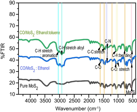
FTIR spectra of MoS2 thin-films compared with MoS2 and CO/MoS2 thin-films prepared in different solvents and synthesized by spin coating at a speed of 3000 r.p.m.
3.4 Profilometer thickness measurement
Thickness measurement of films revealed different features of the MoS2, oligomer, and their mixture at different speeds varying from 500 rpm to 4000 rpm. The pure MoS2 showed rough counters and had low thicknesses, as shown in fig. S2.a. It showed an abrupt change in depth, which could be attributed to MoS2 flakes aggregations. On the other hand, oligomer films displayed a smooth contour, as shown in fig.S2.b. The mixture solution coated film showed features of both MoS2 and oligomer profiles. The thickness of composite films were very thick at low speeds and low thickness at high speed, but intermediate between pure oligomer and MoS2. The thickness profile is shown in Fig. S2.(c). Fig. 7 shows the average thickness of the films pure MoS2, oligomer, and blends. The thickness of the film is measured from the Profilometer Thickness Measurement. The inset shows that the thickness of MoS2 and (BECV-DHF)/MoS2 values are consistent with the expected thickness from a few layers of films (a monolayer about 0.65 nm) (Ma and Shi, 2013).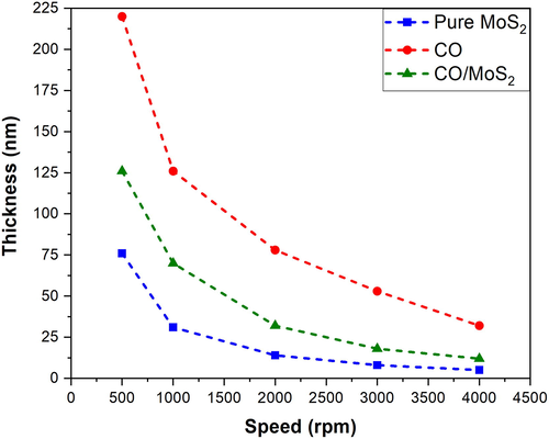
Thickness profile of the films pure MoS2, oligomer, and blends.
3.5 Optical properties
Fig. 8.a shows the normalized absorption spectra of MoS2 films deposited on SiO2/Si substrate dissolved in ethanol obtained by spin coating technique using speed ranging between 500 r.p.m to 4000 r.p.m as a function of photon’s wavelength. For the sake of comparison, the absorption spectrum of one sample of MoS2 dissolved in toluene is also presented in Fig. 8a. The UV–visible absorption spectrum shows three different features around 250, 300, and 750 nm, respectively, which can be ascribed to excitonic transitions. On the first view, one can see that MoS2 thin films could be promising materials for photodetectors and photovoltaic cells (Chen et al., 2016, Shastry et al., 2016,)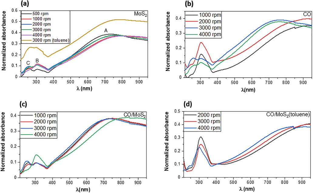
Absorbance spectra of (a) pure MoS2 films, prepared by spin coating and dissolved in ethanol and one sample of MoS2 dissolved in toluene, acquired at different illumination wavelengths (b) the CO BEVC-DHF samples with different speeds (c) CO/MoS2 films dissolved in ethanol and (d) CO/MoS2 films dissolved in toluene. All samples are prepared with different thicknesses and at different speeds varying from 500 to 4000 rpm.
The measurement of optical absorption spectra of pure CO (i.e., BEVC-DHF) thin films prepared at different speed spin coating are presented in Fig. 8.b. It is visible that two weak absorption peaks occur between photons wavelengths of 240 and 340 nm, which are sharpened for samples prepared at low-speed rotations. The absorption spectra have a main peak located approximately at 760 nm for CO thin films prepared at high r.p.m spin-coating speed and 930 nm for CO prepared at low r.p.m spin coating speed. As evident from Fig. 8, the absorption spectra of CO/MoS2 films display a feature analogous to both CO films and MoS2 films at low wavelength radiation regimes prepared at high r.p.m speed. However, the spectral peaks are shifted to high frequency regions for CO/MoS2 films (see Fig. 8c-8d). Comparatively, CO/MoS2 films dispersed in toluene exhibit two spectral peaks, about 4 eV (300 nm) and 1.3 eV (930 nm), respectively, that can be ascribed to interband excitonic transitions. This is due mainly to the energy splitting at the valence band spin − orbit coupling along the k-point of the Brillouin zone (Feng et al., 2016; Paul and Robeson, 2008; Zachariah et al., 2014). Also, the emergence of a strong peak of about 1.77 eV (700 nm) in CO/MoS2 is associated with the π − π transition of the pure CO BEVC-DHF. These results indicate the surface change of MoS2 films with the addition of the conjugate oligomer BEVC-DHF (Fig. 8c- 8d). Moreover, one can see from Fig. 8.c-8.d that the spectral peaks of the samples dissolved in two different solvents have almost the same pattern with weak absorption at low wavelength regimes. Clearly, the s-vacancy is a preferential atomic position for van der Waals interaction from ethanol precursor, and thereby the strong bond is not important in these samples. From the data presented in Fig. 8, the absorption coefficient (
) are determined using the following light attenuation equation (Alwan et al., 2017),
Table 1 summarizes the results of thickness measurements obtained from the profilometer along with absorbance and absorption coefficients for MoS2, CO (BECV-DHF), and CO/MoS2 films. It is evident that increasing coating speed results in a decrease in the thickness of the obtained films. In the case of pure MoS2 films, both the maximum absorbance and absorption coefficient fluctuate between maximum and minimum values with decreasing film thickness. On the other hand, maximum absorbance decreases while the absorption coefficient increases for pure CO (i.e., BECV-DHF) with decreasing film thickness. Interestingly, the maximum absorbance for CO/MoS2 films does not show a wide variation; however, absorption coefficients increase monotonically with decreasing film thickness for this composite. Our optical absorbance results are in good agreement with the previous studies on pentacene/MoS2 and PTB7/MoS2 heterostructures, while the absorption of photons were detected in the UV and IR regions (Jariwala et al., 2016; Lin et al., 2018).
Sample
Speed rotation (rpm)
Film thickness (nm)
Absorbance A
Absorption Coefficient x106 (cm)−1
MoS2
500
76
1.09147
0.330744133
MoS2
1000
31
1.06613
0.792031416
MoS2
2000
14
1.07526
0.17688027
MoS2
3000
8
1.08226
3.11555598
MoS2
4000
5
1.0565
4.866239
CO
1000
126
1.16242
0.212464544
CO
2000
78
1.13669
0.335615009
CO
3000
53
1.11488
0.484446913
CO
40,000
32
1.08271
0.779212853
CO/ MoS2
10,000
70
1.09152
0.35911008
CO/ MoS2
2000
32
1.09148
0.785524513
CO/ MoS2
3000
18
1.08079
1.38281076
CO/ MoS2
4000
12
1.10575
2.12211854
In Fig. 9, both the layered structure and energy level diagram of solar cells are shown. The energy level of BECV-DHF is obtained using TD-DFT simulation using gaussian software following simulation procedure reported previously (Aljaafreh et al., 2019). The addition of MoS2 induces a heterogenous interface, the CO absorption is in UV and blue region with very high quantum efficiency. The CO absorbed photons create tightly bounded excitons when these excitons migrate to the interface of MoS2 nanoflakes. Due to the potential gradient, the exciton splits into electron and hole, thus producing a photovoltaic current. This connectivity of oligomer is amorphous and have a low conductivity. But when dissolved in solvents like toluene and spin coated at speed 1000–3000 rpm, they form self-assembled nano crystals and these crystal domains behave as a semiconductor. At high speed, the CO thin films become amorphous (Aljaafreh et al., 2019; AlSalhi et al., 2020). The formation of nano crystals CO on top of MoS2 is confirmed by SEM and TEM analysis as shown in Fig. 3. This nanostructure could be attributed to the photovoltaic behavior of CO/MoS2. Different configuration of solar devices was designed, for each configuration 20 devices. The I-V and IPEC characteristic parameters of device (a-f) configuration are given in Fig. 9b and 9c respectively. The parameters of devices (a) – (f) are given in Table 2.
Device ID
Structure
PCE (%)
Jsc (mA)
Voc (V)
FF (%)
IV
IPCE
(a)
ITO/MoS2/Ca/Al
–
–
–
–
–
(b)
ITO/BECV-DHF/Ca/Al
0.98
3.33
3.36
0.63
0.467
(c)
ITO/PEDOT:PSS/MoS2/Ca/Al
1.95
5.313
5.266
0.626
0.584
(d)
ITO/PEDOT:PSS/BECV-DHF:MoS2/Ca/AlBECV-DHF:MoS2 layer (1000 rpm)
4.88
12.59
12.61
0.64
0.602
(e)
ITO/PEDOT:PSS/BECV-DHF:MoS2/Ca/AlBECV-DHF:MoS2 layer (2000 rpm)
5.86
14.7
14.59
0.642
0.62
(f)
ITO/PEDOT:PSS/BECV-DHF:MoS2/Ca/AlBECV-DHF:MoS2 layer (3000 rpm)
3.84
10.4
10.53
0.63
0.57
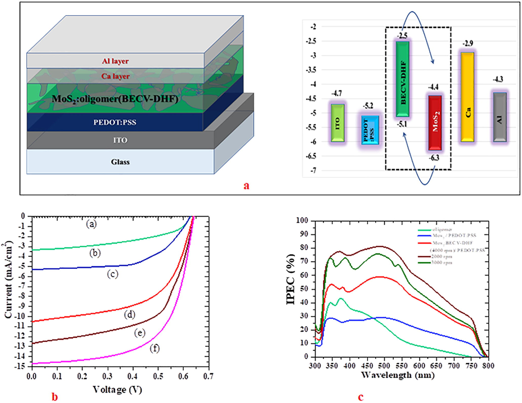
The device configuration (a) was ITO/MoS2/Ca/Al and it is not active and serves as reference. Next, the device configuration (b) was ITO/BECV-DHF/Ca/Al has fill factor (FF) of 0.467, power conversation efficiency (PCE) was 0.98. It is imperative to give an additional layer of electron conductive layer, hence a layer of PEDOT:PSS was coated on top ITO to form a device (c) with configuration, ITO/PEDOT:PSS/MoS2/Ca/Al which had PCE of 1.95%, FF of 0.587. Next the performance of device configurations (d) to (f) had following layers ITO/PEDOT:PSS/BECV-DHF:MoS2/Ca/Al, but the BECV-DHF:MoS2 composite based active layer thickness is varied by coating at different spin speeds. The device (e) gave the maximum PCE of 5.86% and higher FF of 0.62, due to the formation of BECV-DHF nanocrystals on MoS2. But when the speed increases to 3000 rpm or higher, the efficiency drops, i.e PCE of 3.84% (device (f)). The reduction in PCE and FF at higher speed could be due to the fact that BECV-DHF do not form crystal and becomes amorphous with very high impedance (AlSalhi et al., 2020). Thus reducing the PCE dramatically.
We are encouraged by previous reports on MoS2 based memory device (Zhang et al., 2013), hence examined the possiblity of BECV-DHF:MoS2 composite based memory device. The memory device takes advance of amorphous nature of BECV-DHF at high speeds, to attain sufficient cover throughout and uniformity five layers of BECV-DHF:MoS2 composite was spin coated. The I-V characteristics was measured with forward and reverse sweep from −6 V to 6 V. During the forward sweep 0 – 6 V, a power surge was observed as shown in Fig. 10.(b). The Fig. 10. (c)(ii), shows a linear increase of ln (I) with respect to
at region I, indicating that the underlying mechanism is thermionic emission. The device could retain the 70% performance even after 1000 sweeps. The device is flexible without losing its ductility until 2000 pressing. The Fig. 10 (c) (ii) shows the off state and Fig. 10 (c) (iii) shows the dramatic change in the slope from 2 to 43.3 indicating the resistive switching.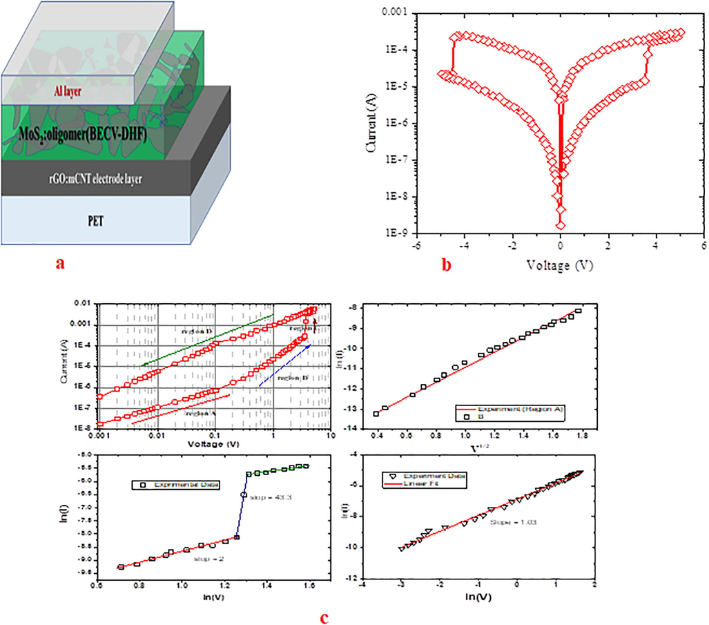
(a) schematic of memory device; 10.(b) I–V characteristics of memory device; (c).(i) The trace of current as a function of invoked voltage for the flexible memory device in voltage range from 0 to +5 (+ve sweep). Experimental data and fitted lines of the ln(I)–ln(V) characteristics in region A and region B in the OFF state, region C and region D is the resistive switching and the ON state. (c).(ii) linear plot of ln (I) vs V1/2 at region A; (c).(iii) and (iv). the plot of ln(I) vs ln(V) in region B and C.
4 Conclusions
In this research paper, the modification of morphology of MoS2, CO (BECV-DHF), and CO/MoS2 films of different thicknesses synthesized on SiO2/Si substrate using spin coating technique by employing SEM, TEM and XRD. Accordingly, the synthesized MoS2-thin film are found to be dispersed homogeneously. The optical absorbance spectra of MoS2, CO, and CO/MoS2 films are probed in a relevant portion of electromagnetic spectra ranging between 250 nm (UV) and 1000 nm (NIR). Profilometer measurements were performed to determine the thickness of MoS2, CO, and CO/MoS2 films, while XPS fingerprint was used to evaluate the compositional elements of synthesized samples along with electronic states of elements interacting with Mo at specific binding energy peaks. Our results indicate that the CO/MoS2 composite films can be a fascinating candidate for electronic applications, such as Zener transistors devices. In particular, the fabricated solar cell and memory device studied showed promising results. A PCE of 5.8% was achieved for solar cell. The memory device also showed switching and charge retention behavior as desired. Our results indicate that CO/MoS2 can be suitable for diode device applications because of the polarization of carrier charge transport, and this can eventually imply p-n junctions. The interesting optical and electrical properties could be attributed to the formation of CO nanocrystals on MoS2.
Acknowledgements
The authors are grateful to the Deanship of Scientific Research, King Saud University for funding through Deanship of Scientific Research Chairs.
Declaration of Competing Interest
The authors declare that they have no known competing financial interests or personal relationships that could have appeared to influence the work reported in this paper.
References
- Abdulaziz Alfahd, S., Prasad, S., Al-Mujammi, W., Devaraj, D., Masilamani, V., AlSalhi, M.S. An Efficient Violet Amplified Spontaneous Emission (ASE) from a Conjugated Polymer (PFO-co-pX) in Solution. Materials (Basel).10(2017), pp. 265. 10.3390/ma10030265.
- Optically pumped intensive light amplification from a blue oligomer. Polymers (Basel). 2019;11:1534.
- [CrossRef] [Google Scholar]
- Narrowband spontaneous emission amplification from a conjugated oligomer thin film. Polymers (Basel). 2020;12:232.
- [CrossRef] [Google Scholar]
- AlSalhi, M.S., Almotiri, A.R., Prasad, S. Aljaafreh, M.J., Othman, A.H.M. Masilamai, V. A Temperature-Tunable Thiophene Polymer Laser. Polymers (Basel).10(2018), pp. 470. 10.3390/polym10050470.
- Alwan, T.J., Mkhaiber, A. F., Hussein, A.F., Khaleel, R.I., Mohi, A.T. Effect of neutron-irradiation on the optical properties of PVA/K2CrO4 composites. 2(2017), pp. 31-34.
- MoS2–Gd chelate magnetic nanomaterials with core-shell structure used as contrast agents in in vivo magnetic resonance imaging. ACS Appl. Mater. Interfaces.. 2016;8:1827-1835.
- [CrossRef] [Google Scholar]
- Polymer-II-VI nanocrystals blends: basic physics and device applications to lasers and LEDs. Nanomaterials (Basel). 2019;9:1036.
- [CrossRef] [Google Scholar]
- Solution-processed two-dimensional metal dichalcogenide-based nanomaterials for energy storage and conversion. Adv. Mater.. 2016;28:6167-6196.
- [CrossRef] [Google Scholar]
- Templating C60 on MoS2 Nanosheets for 2D Hybrid van der Waals p–n Nanoheterojunctions. Chem. Mater.. 2016;28:4300-4306.
- [CrossRef] [Google Scholar]
- Choi, W., Cho, M.Y., Konar, A., Lee, J.H., Cha, G.B., Hong, S.C., Kim, S., Kim, J., Jena, D., Joo, J., Kim, S. High-detectivity multilayer MoS(2) phototransistors with spectral response from ultraviolet to infrared. Adv Mater. 24(2012), pp.5832-6. 10.1002/adma.201201909.
- Chu, X.S., Yousef, A., Li, D.O., Tang, A.A., Duo Ma, A.D., Green, A.A., Santos, E.J.G., Wang, Q.H. Direct Covalent Chemical Functionalization of Unmodified Two-Dimensional Molybdenum Disulfide. Chem. Mater. 30(2016), pp. 2112–2128. 10.1021/acs.chemmater.8b00173.
- Collins, C.B., Tofanelli, M.A., Crook, M.F., Phillips, B.D. Ackerson CJ. Practical Stability of Au25(SR)18-1/0/+1. RSC Adv. 7(2017), pp. 45061-45065. 10.1039/C7RA07511A.
- Two-dimensional transition metal dichalcogenides as atomically thin semiconductors: opportunities and challenges. Chem. Soc. Rev.. 2015;44:8859-8876.
- [CrossRef] [Google Scholar]
- Defect-free MoS2 nanosheets: advanced nanofillers for polymer nanocomposites. Compos. Part A-Appl. S. 2016;81:61-68.
- [CrossRef] [Google Scholar]
- Dynamics of chemical vapor sensing with MoS2 using 1T/2H phase contacts/channel. Nanoscale. 2016;8:11445-11453.
- [CrossRef] [Google Scholar]
- Hybrid, gate-tunable, van der waals p-n heterojunctions from pentacene and MoS2. Nano Lett.. 2016;16:497-503.
- [CrossRef] [Google Scholar]
- Sonolytic doping of poly (1-naphthylamine) with luminol: influence on spectral, morphological and fluorescent characteristics. Colloid Polym. Sci.. 2017;295:715-724.
- [CrossRef] [Google Scholar]
- Measurement of the elastic properties and intrinsic strength of monolayer graphene. Science. 2008;321:385-388.
- [CrossRef] [Google Scholar]
- Thermal Evaporation Deposition of Few-layer MoS2 Films. Nano-Micro Lett.. 2013;5:135-139.
- [CrossRef] [Google Scholar]
- Milad, R., Shi, J., Aguirre, A., Cardone, A., Medina, B.M., Farinola, G. M., Abderrabba, M., Gierschner, J. Effective conjugation in conjugated polymers with strongly twisted backbones: a case study on fluorinated MEHPPV. 4 (2016), pp. 6900–6906.10.1039/C6TC01720G.
- Riaz, U., Ashraf, S.M., Aleem, S., Budhiraja, V., Jadoun, S. Microwave-assisted green synthesis of some nanoconjugated copolymers: characterisation and fluorescence quenching studies with bovine serum albumin. New J. Chem., 40 (2106), pp. 4643-4653. 10.1039/C5NJ02513C.
- Influence of Luminol Doping of Poly(o-phenylenediamine) on the spectral, morphological, and fluorescent properties: a potential fluorescent marker for early detection and diagnosis of Leishmania donovani. ACS Appl. Mater. Interfaces. 2017;9:33159-33168.
- [CrossRef] [Google Scholar]
- Layered semiconductor molybdenum disulfide nanomembrane based Schottky-barrier solar cells. Nanoscale. 2012;4:7399-7405.
- [CrossRef] [Google Scholar]
- Mutual photoluminescence quenching and photovoltaic effect in large-area single-layer MoS2-polymer heterojunctions. ACS Nano. 2016;10:10573-10579.
- [CrossRef] [Google Scholar]
- Syari’ati, A., Kumar, S., Zahid , A., Ali El Yumin, A., Ye, J., Rudolf, P. Photoemission spectroscopy study of structural defects in molybdenum disulfide (MoS2) grown by chemical vapor deposition (CVD). Chem Commun (Camb). 55(2019), pp.10384-10387. 10.1039/c9cc01577a.
- Vertical cavity lasing from melt-grown crystals of cyano-substituted thiophene/phenylene co-oligomer. Appl. Phys. Lett.. 2015;107:163303-163307.
- [CrossRef] [Google Scholar]
- Xu, X.Y. Yin, Z.Y., Xu, C.X., Dai, J. Hu, J.G. Resistive switching memories in MoS2 nanosphere assemblies. Appl. Phys. Lett. 104(2014) 033504; 10.1063/1.4862755.
- Highly scalable synthesis of MoS2 thin films with precise thickness control via polymer-assisted deposition. Chem Mater. 2017;29(14):5772-5776.
- [CrossRef] [Google Scholar]
- Preparation and enhancement of thermal conductivity of heat transfer oil-based MoS2 nanofluids. Nanomaterials. 2013;2013:1-6.
- [CrossRef] [Google Scholar]
- Rheological behaviour of clay incorporated natural rubber and chlorobutyl rubber nanocomposites. RSC Adv.. 2014;4:58047-58058.
- [CrossRef] [Google Scholar]
- Nonvolatile rewritable memory device based on solution-processable graphene/poly(3-hexylthiophene) nanocomposite. Mater. Chem. Phys.. 2013;142:626-632.
- [CrossRef] [Google Scholar]
Appendix A
Supplementary data
Supplementary data to this article can be found online at https://doi.org/10.1016/j.jksus.2021.101389.
Appendix A
Supplementary data
The following are the Supplementary data to this article: