

Synthesis and characterization of SnO2 thin films using metalorganic precursors
⁎Corresponding author. tjen@uj.ac.za (Tien-Chien Jen)
-
Received: ,
Accepted: ,
This article was originally published by Elsevier and was migrated to Scientific Scholar after the change of Publisher.
Peer review under responsibility of King Saud University.
Abstract
Abstract
Tetrakis (dimethylamino) tin(IV) (TDMASn) is a metal organic precursor used for fabricating transparent conducting tin oxide (SnO2) thin films via atomic layer deposition process (ALD). This study reported for the first time, a spin coating fabrication process of transparent conducting SnO2 thin films using TDMASn as the precursor for electrode materials of solar cells substrate. The samples were prepared using sol–gel spin-coating process and annealed at different temperatures to form metastable crystal structured SnO2 thin films. The manufactured thin films consequently underwent X-ray diffraction (XRD), scanning electron microscope (SEM), UV–vis spectroscopy, and resistivity analysis. The XRD analysis certified the films to be of polycrystalline structure, with the SEM results revealing variations in film thicknesses. The UV–vis analysis demonstrated a peak absorption band at 250 nm, while the highest transmittance of 83.2% in the visible range was noticed at the 550 °C sample.
Keywords
Tin oxide
Thin films
Spin-coating

1 Introduction
SnO2 is an essential n-type semiconductor that has a broad bang gap of 3.6 eV. It also possesses features of high transparency and infrared reflectivity, with high resistance towards moisture and acid (Martinez-Gazoni et al., 2018). SnO2 alongside doped SnO2 has comprehensively been researched in recent times because of its optical properties in addition to its high load carrier mobility and density.
Transparent conductive oxides (TCO) display a phenomenal blend of near-metallic conductivity, high reflectivity in the infrared light region, and high transmittance in the region of visibility (Sunde et al., 2012). Due to their distinctive features, TCOs are applied in a wide range of technological applications like light-emitting diodes flat panel displays, photovoltaic devices, energy-efficient windows, touch panels, and gas sensors (Abdelghani et al., 2019). Indium tin oxide (ITO) has been the TCO material utilized as a layer in the majority of optoelectronic applications, however, owing to its exorbitant price and scarcity, an alternative was sought to succeed the ITO which resulted in the discovery of SnO2 (Kadhim and Abu Hassan, 2017). The SnO2 group is among the semiconductors of metal oxides that are appropriate to be implemented as TCO due to their outstanding qualities. When used as a chemical material, they are just about the only pure semiconductors which have low-temperature properties for film deposition, ideal precursors, and outstanding manufacturing performance (Giraldi et al., 2006). When utilized as an electrical material they possess superior electrical conductivity as an n/p type semiconductor, as well as carrier mobility (Das and Jayaraman, 2014). They also are studied as mechanical materials in an acidic or basic medium, eco-friendly, and suitable for minimal vacuum deposition with easy morphology and composition control. As a commercial material, they are very affordable and readily available for wide areas with the doping level being easily controlled, and as optical materials, the visible-near infrared region has high transmittance to reflectance (Bhat et al., 2006). Therefore, the SnO2 material is regarded to have been established as a TCO across every area of application.
In film fabrication, the different deposition techniques play crucial roles in the behavior of the films (Nwanna et al., 2020). The distinct manufacturing processes of SnO2 thin films are RF sputtering, photochemical deposition, dip coating and spin-coating sol–gel processes, chemical vapor deposition, and spray pyrolysis (Nwanna et al., 2020), with each of these methods having their merits and demerits. The spin-coating deposition process also known as a solution-based approach is an efficient and straightforward process that utilizes two-dimensional substrates for the deposition of uniform thin films (Kim et al., 2014). Regarding large-scale electronic applications, solution-based techniques are chosen over vapor phase procedures, not necessarily because of their simple structure, but because of their highly controllable ambient processing and their low costs (Gu et al., 2004).
It has been reported that SnO2 thin films produced through the spin-coating process can be utilized as solar cell electrode materials, and spectroscopic gas sensors (Kolmakov et al., 2003), thus there have been various works regarding the deposition of SnO2 thin films via the spin coating process using various precursors. However, to the best of our knowledge, there have been no reports on the fabrication of SnO2 films via spin coating using TDMASn as precursor. Therefore, this study is performed with keen interest to analyze the synthesis, fabrication, and properties of the fabricated spin-coating SnO2 thin films from TDMASn.
2 Experimental method
2.1 Materials
The materials utilized in performing the experimental analysis consists of, 1-butanol (99.8%), methanol (99.6%), ethanol (99.9%), nitric acid (HNO3) (70%), acetone (90%), tetrakis (dimethylamino) tin(IV) (TBMASn), silicon glass substrate, and fluorine tin oxide (FTO) glass substrate were procured from Sigma-Aldrich. The chemicals purchased were used as supplied.
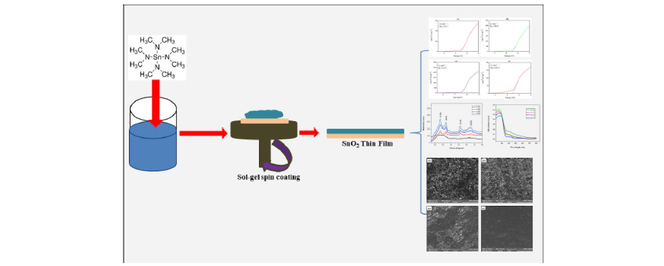
2.2 Preparation
A solution of 0.22 mol of 1-butanol and 0.019 mol of nitric (HNO3) acid was prepared. Afterward, 1 g (0.00339 mol) of tetrakis (dimethylamino) tin(IV) was dissolved in the solution and stirred at 200 rpm for 24hrs at room temperature to form a sol–gel. The gel solution was then spin-coated on the glass substrate at 3000 rpm for 30 s in ambient condition to form the thin films. Afterward, the substrate dried at 100 °C for 60 s to remove the leftover butanol. The various thin films deposited on the substrate were then distinctively annealed for 3 h at 250 °C, 350 °C, 450 °C, and 550 °C in a muffle furnace under nitrogen flow.
2.3 Materials characterization & procedures
The elemental analysis and surface structure of the fabricated thin films were analysed with SEM/EDS (TESCAN VEGA 3 TC SEM, attached with Oxford Energy Dispersive Spectrometer). The samples were first coated with carbon before inserting into the instrument. The XRD analysis which was executed with the “PANalytical X’Pert PRO X-ray Diffractometer using Cu radiation with K Beta filter” was applicable in deducing the structural properties of the fabricated film. The deposited samples were cut to size to fit into the instrument holder. The UV-1800 spectrophotometer measured the UV absorbance and transmittance of light on the formed thin film. Here a baseline procedure was first conducted on the instrument before the introduction of the samples for realization of accurate test results. While the film’s resistivity was derived using the Four Probe-Resistivity Measurement (SK012). In this test, the four pointers of the instrument were placed on the samples at room temperature and the different electrical readings obtained.
3 Results and discussion
3.1 Structural analysis
Fig. 1 demonstrates the XRD pattern of the SnO2 thin films fabricated at varying calcining temperatures. The deposited films were polycrystalline except the 250 °C sample which possessed an amorphous structure (Choi et al., 2014). This was because of its reduced calcination temperature hence no diffraction peaks were observed. Reduced annealing temperatures result in more chemical compounds, reduced film stoichiometry, increased impurity fusion, and defective crystallinity (Rahal et al., 2015). Notwithstanding, all these qualities can be enhanced with an increment in the annealing temperature, as higher calcination temperatures result in an increased film stoichiometry. Thus, with a subsequent increase in the annealing temperature, the peaks at (1 1 0), (1 0 1), and (2 1 1) became visible as seen in the 350 °C and 450 °C samples of Fig. 1. These peaks correspond to the orthorhombic structure of SnO2 thin films (JCPDS card no.04-015-3276) (Barakat et al., 2018). A further elevation to 550 °C generated an increased XRD peak intensity for the deposited SnO2 films, with an additional peak (1 1 2) being also recognized (Jeong et al., 2006). At the 550 °C annealing temperature, the film transformed to a tetragonal phase (JCPDS card no. 04-012-0771) (Liu et al., 2010). Furthermore, the crystallite size D (nm) which is known as the littlest single crystal in the powdered form of materials, was calculated from Scherer's equation and shown in Table 1. It was observed that the crystallite size and the d-spacing of the fabricated thin films decreased with increasing annealing temperature (Sayeed and Rouf, 2021). These findings affirm that superior SnO2 thin films are fabricated at higher calcining temperatures which corroborates the result from the elemental composition characterization.
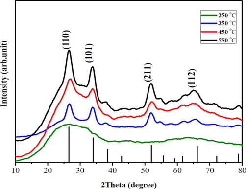
- XRD of the fabricated SnO2 thin films at varying temperatures.
| Calcination Temperature (oC) | d-spacing | Crystallite Size (nm) |
|---|---|---|
| 250 | Amorphous | Amorphous |
| 350 | 2.613471 | 0.772 |
| 450 | 2.613455 | 0.743 |
| 550 | 2.613421 | 0.716 |
3.2 Morphological analysis
The SEM images from Fig. 2 illustrate the similitudes among the films which consisted of nanometric agglomerated spherical particles of structured shapes and sizes (Fernandes et al., 2019). The SEM micrograph from Fig. 2a (250 °C,) indicated the film consisted of reduced particle sizes of 16.04 nm (Choudhary et al., 2013). However, an increase in the annealing temperature from 350 °C to 450 °C, brough about an increase in the film’s particle size from 18.56 nm to 19. 47 nm (Fig. 2b-c). Furthermore, the 550 °C sample exhibited a particle size of 21.55 nm (Choudhary et al., 2013) as demonstrated in Fig. 2d. This is because an increase in the annealing temperature led to an increase in the film’s crystallinity thus increasing the crystallites quantity (Valladares et al., 2012). It was however concluded that the average size of the films and their morphologies increased with increasing calcination temperature. This agreed with the preceding study of Palanichamy et al (2018), which also had their films acquiring comparable shapes. Also, the film thickness of the fabricated SnO2 thin films were evaluated with the Swanopoel Envelope method (Chaitra et al., 2016). The obtained thicknesses were 407.51 nm at 250 °C, 405.77 nm at 350 °C, 403.58 nm at 450 °C, and 400.01 nm at 550 °C respectively, which consequently agreed with the structural characterization of the produced film (Roy et al., 2018).
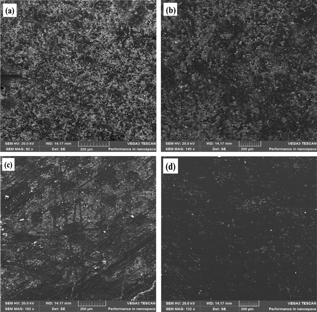
- SnO2 SEM micrographs at (a), 250 °C (b), 350 °C (c) 450 °C (d) 550 °C.
3.3 Elemental analysis
The elemental composition of the thin films were analyzed using the energy-dispersive X-rays (EDX). A silicon (Si) peak was noticed in Fig. 3 due to Si present in the substrate (glass) utilized in the deposition procedure (Ergin et al., 2009). However, clear and accurate peaks pertaining to Sn and O were also detected in the spectrum of the SnO2 thin film annealed at different temperatures (Fig. 3a-d). This outcome thus indicates that the manufactured thin films were comprised of only tin and oxygen elements with very few impurities, which correctly aligned to the structural aspect of the films. Also, the percentage weight of Sn in the SnO2 thin film improved with increasing annealing temperature, which therefore implied that higher annealing temperature favored the production of the SnO2 compound (Wongsaprom et al., 2014).
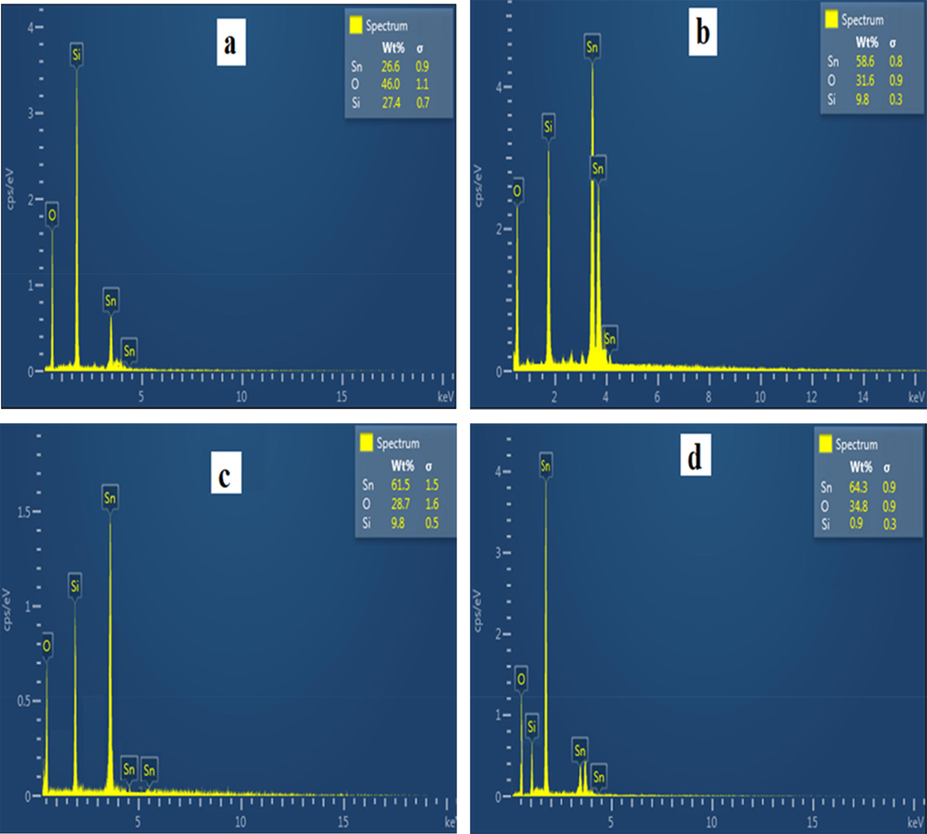
- EDX spectrum at (a), 250 °C (b), 350 °C (c) 450 °C (d) 550 °C.
3.4 UV–vis absorbance
The optical properties which were measured by the UV-1800 spectrophotometer display the optical absorbance spectra of tin oxide thin film with varying annealing temperatures of 250, 350, 450, and 550 °C, respectively. A wavelength in the range of 200–800 nm was used to dispatch the photon for analyzing the absorption spectra. The absorption coefficient of the thin films (Fig. 4) is higher in the UV region than in the visible light region (Kamble et al., 2017). The absorbance curve which possesses three regions has its first region between the range of 800 nm to 370 nm where there is fluctuation in the absorbance. The second wavelength region of 370 nm to 250 nm had a surge in the absorbance curve up to the maximum peak absorbance at 250 nm, while the third region of 240 nm to 215 nm has the absorbance curve dropping (Razeghizadeh et al., 2015). An absorption edge of 280 nm was observed for the fabricated thin films. Consequently, Fig. 4 indicated that the peak absorbance of the deposited thin films decreased in wavelength with increasing annealing temperature. This was a result of the collision profile being narrowed (Molloy and Holcombe, 2006).
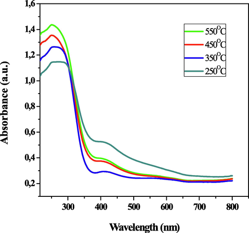
- The UV–vis absorbance spectra of the SnO2 thin films at various temperatures.
3.5 Band gap
It is known that the theory of optical absorption provides the relationship between the absorption coefficients (α) and the photon energy (hν). The optical energy band gap is however determined by; (Kamble et al., 2017).
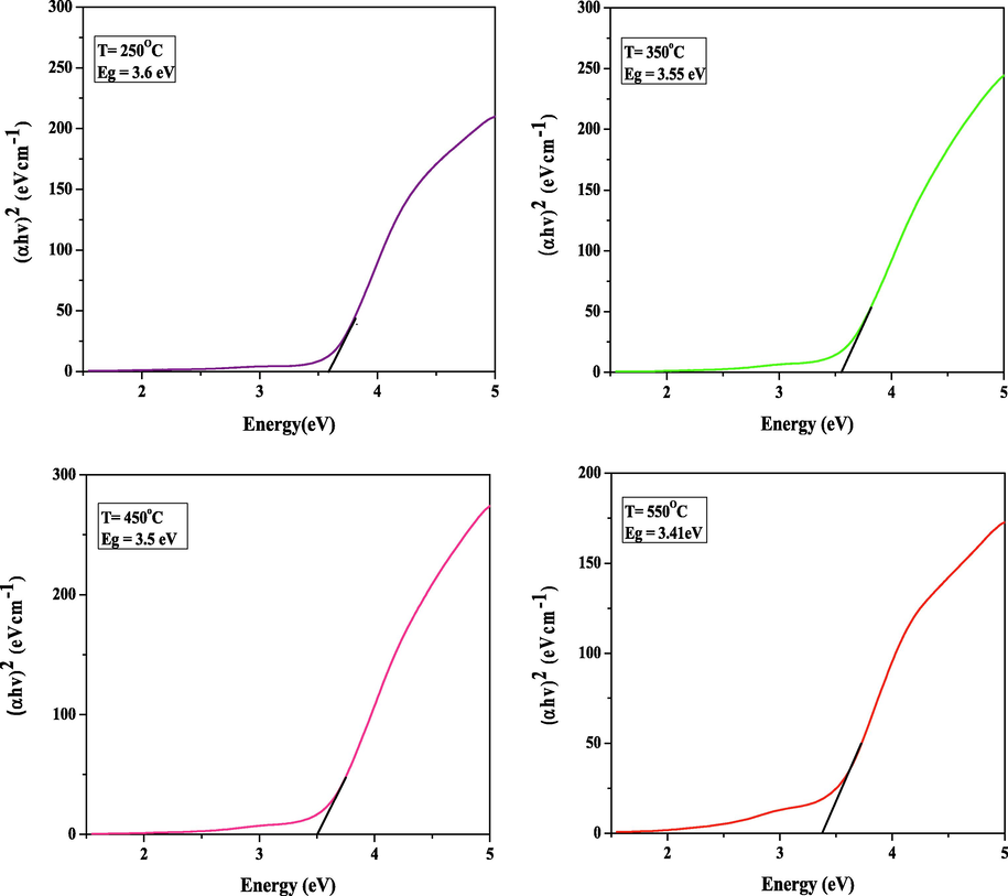
- The bandgap of SnO2 thin film at distinct temperatures.
3.6 Transmittance
It is generally known that thin films transmittance is influenced by the bandgap energy, film crystallinity, and surface morphology (Choi and Park, 2014). Also, materials which have broad energy band gaps maintain superior transmittance. Fig. 6 illustrates the spectra of optical transmittance of the deposited SnO2 thin films annealed within the temperatures of 250 °C to 550 °C in a solution concentration of 1.745 g/cm3. Excerpt from the figure indicated that at increased calcining temperatures, the mean transmittance of the spin-coated SnO2 films in the spectra region of visibility, increased from approximately 63.5% to 83.2% at a wavelength of 500 nm following an adsorption edge at the 350 nm region. This reduction in transmittance with increasing calcination temperature can be as a result of high mobility charge carriers, along with the reduction of free carrier absorption (Usha et al., 2015). Higher calcination temperatures produce finer film surfaces, resulting in lower scattering effects, as well as a resultant increase in the optical transmittance (Zadsar et al., 2012).Fig. 7..
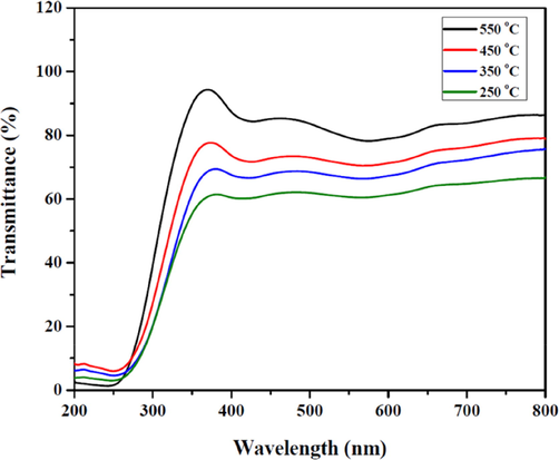
- The UV–vis transmittance spectra of the calcined SnO2 thin films at different temperatures.
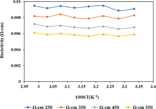
- SnO2 thin film resistivity at varying temperatures.
3.7 Resistivity
The resistivity of the SnO2 thin films were measured with the four-point probe and plotted as a function of temperature. This analysis demonstrated a continuous decrease in the SnO2 thin films resistivity with increasing calcination temperatures (Elam et al., 2008). The reduction in the film resistivity with a respective increment in the annealing temperature is attributed to the improvement in film crystallinity and structural differences, which could impair the film's electrical resistivities (Khan et al., 2010). The 550 °C calcination temperature possessed lower resistivity, whereas the 450 °C and 350 °C temperatures maintained moderate resistivities, with the 250 °C temperature having the highest resistivity. Consequently, the recognised resistivity pattern in this work affirmed the semiconducting behavior of the fabricated SnO2 thin films, which emulated similar trends from prior studies (Senthilkumar and Vickraman, 2010). Thus, it could be said that increased calcination temperatures support the conductivity of semiconductors since it decreases their resistivity.
4 Conclusion
Metastable tetragonal SnO2 thin films have been prepared on glass substrates at distinct annealing temperatures using a novel production procedure for TDMASn. The outcome of the structural results reported the films to be preferentially adapted towards the (1 1 0), (1 0 1), (2 1 1), and (1 1 2) directions for each of the samples, with the 550 °C sample having the highest peak and the 250 °C sample having no peak due to its low calcination temperature. Consequently, the existence of nanosized SnO2 thin films was established from the morphological results. Also, the film's band gap values were in relation to those reported in preceding works. Maximum absorbance as well as peak transmittance at 250 nm and 83.2% respectively were attained only at the 500 °C sample. Thus, the derived results go a long way to indicate that superior SnO2 thin films are formed at higher annealing temperatures.
Conflicts of interest
The authors declare no conflicts of interest.
CRediT authorship contribution statement
Emeka Charles Nwanna: Formal analysis, Data curation. Patrick Ehi Imoisili: Methodology, Investigation. Tien-Chien Jen: Conceptualization, Funding acquisition, Resources.
Declaration of Competing Interest
The authors declare that they have no known competing financial interests or personal relationships that could have appeared to influence the work reported in this paper.
References
- Nano-architecture of highly sensitive SnO2–based gas sensors for acetone and ammonia using molecular imprinting technique. Sensors Actuat. B:Chem.. 2019;297:126668
- [CrossRef] [Google Scholar]
- Structural, ultrasonic and spectroscopic studies of tin oxide thin films; effect of Ir and (Ni, Ir) double doping. Mater. Res. Express. 2018;5(6):066407
- [CrossRef] [Google Scholar]
- Influence of Zn doping on electrical and optical properties of multilayered tin oxide thin films. Bull. Mater. Sci.. 2006;29(3):331-337.
- [CrossRef] [Google Scholar]
- Structural and photoluminescence properties of tin oxide and tin oxide: C core–shell and alloy nanoparticles synthesized using gas phase technique. AIP Adv.. 2016;6(9):095321
- [CrossRef] [Google Scholar]
- Dependence of solution molarity on structural, optical and electrical properties of spin coated ZnO thin films. J. Mater. Sci.: Mater. Electron.. 2016;27(7):7614-7621.
- [CrossRef] [Google Scholar]
- Highly conductive SnO2 thin films deposited by atomic layer deposition using tetrakis-dimethyl-amine-tin precursor and ozone reactant. Surf. Coat. Technol.. 2014;259:238-243.
- [CrossRef] [Google Scholar]
- Choi D.-w., Maeng W., Park J.-S. 2014. The conducting tin oxide thin films deposited via atomic layer deposition using Tetrakis-dimethylamino tin and peroxide for transparent flexible electronics. Appl. Surf. Sci. 313, 585-590. .
- Effect of processing on the particle size of tin oxide nano-powders. J. Mater. Sci.: Mater. Electron.. 2013;24(2):752-757.
- [CrossRef] [Google Scholar]
- SnO2: A comprehensive review on structures and gas sensors. Prog. Mater Sci.. 2014;66:112-255.
- [CrossRef] [Google Scholar]
- Atomic layer deposition of indium tin oxide thin films using nonhalogenated precursors. J. Phys. Chem. C. 2008;112(6):1938-1945.
- [CrossRef] [Google Scholar]
- Characterization of ZnO films obtained by ultrasonic spray pyrolysis technique. Int. J. Hydrogen Energy. 2009;34(12):5249-5254.
- [CrossRef] [Google Scholar]
- Exploring the properties of niobium oxide films for electron transport layers in perovskite solar cells. Front. Chem.. 2019;7:50.
- [CrossRef] [Google Scholar]
- Deposition of controlled thickness ultrathin SnO2: Sb films by spin-coating. J. Nanosci. Nanotechnol.. 2006;6(12):3849-3853.
- [CrossRef] [Google Scholar]
- Luminescence of SnO2 thin films prepared by spin-coating method. J. Cryst. Growth. 2004;262(1–2):182-185.
- [CrossRef] [Google Scholar]
- Structural and optical properties of SnO2 thin films deposited by using CVD techniques. J. Korean Phys. Soc.. 2006;48(5):960-963.
- [Google Scholar]
- Effect of aging heat time and annealing temperature on the properties of nanocrystalline tin dioxide thin films. Mod. Phys. Lett. B. 2017;31(12):750114
- [CrossRef] [Google Scholar]
- Characterization and NO2 gas sensing properties of spray pyrolyzed SnO2 thin films. J. Anal. Appl. Pyrol.. 2017;127:38-46.
- [CrossRef] [Google Scholar]
- Characteristics of electron beam evaporated nanocrystalline SnO2 thin films annealed in air. Appl. Surf. Sci.. 2010;256(7):2252-2258.
- [CrossRef] [Google Scholar]
- Review of solution-processed oxide thin-film transistors. Jpn. J. Appl. Phys.. 2014;53(2S):02BA02.
- [Google Scholar]
- Detection of CO and O2 using tin oxide nanowire sensors. Adv. Mater.. 2003;15(12):997-1000.
- [CrossRef] [Google Scholar]
- First-principles calculations of structural, electronic and optical properties of tetragonal SnO2 and SnO. Comput. Mater. Sci.. 2010;47(4):1016-1022.
- [CrossRef] [Google Scholar]
- Conductivity and transparency limits of Sb- doped Sn O 2 grown by molecular beam epitaxy. Phys. Rev. B. 2018;98(15)
- [CrossRef] [Google Scholar]
- Detection of palladium by cold atom solution atomic absorption. Anal. Chem.. 2006;78(18):6634-6639.
- [CrossRef] [Google Scholar]
- Fabrication and synthesis of SnOX thin films: a review. Int. J. Adv. Manuf. Technol.. 2020;111(9–10):2809-2831.
- [CrossRef] [Google Scholar]
- Physical properties of nebulized spray pyrolysised SnO2 thin films at different substrate temperature. Appl. Phys. A. 2018;124(9):1-13.
- [CrossRef] [Google Scholar]
- Structural, optical and electrical properties studies of ultrasonically deposited tin oxide (SnO2) thin films with different substrate temperatures. Superlattices Microstruct.. 2015;86:403-411.
- [CrossRef] [Google Scholar]
- Razeghizadeh A.R., Zalaghi L., Kazeminezhad I., and Rafee V., 2015. Effects of sol concentration on the structural and optical properties of SnO2 nanoparticle. arXiv preprint arXiv:1502.00219.
- Relation between the thermal conductivity and grain size in a polycrystalline silicene sheet. In: Paper Presented at the AIP Conference Proceedings. 2018.
- [CrossRef] [Google Scholar]
- Structural, optical and electrical studies on nanocrystalline tin oxide (SnO2) thin films by electron beam evaporation technique. J. Mater. Sci.: Mater. Electron.. 2010;21(6):578-583.
- [CrossRef] [Google Scholar]
- Al-doped SnO2 thin films: impacts of high temperature annealing on the structural, optical and electrical properties. J. Mater. Res. Technol.. 2021;15:3409-3425.
- [CrossRef] [Google Scholar]
- Transparent and conducting ITO thin films by spin coating of an aqueous precursor solution. J. Mater. Chem.. 2012;22(31):15740-15749.
- [CrossRef] [Google Scholar]
- Niobium pentoxide (Nb2O5) thin films: rf power and substrate temperature induced changes in physical properties. Optik-Int. J. Light Electron Optics. 2015;126(19):1945-1950.
- [CrossRef] [Google Scholar]
- Crystallization and electrical resistivity of Cu2O and CuO obtained by thermal oxidation of Cu thin films on SiO2/Si substrates. Thin Solid Films. 2012;520(20):6368-6374.
- [CrossRef] [Google Scholar]
- Principles of chemical bonding and band gap engineering in hybrid organic–inorganic halide perovskites. J. Phys. Chem. C. 2015;119(11):5755-5760.
- [CrossRef] [Google Scholar]
- Synthesis and characterization of tin oxide (SnO2) nanocrystalline powders by a simple modified sol–gel route. Appl. Phys. A. 2014;114(2):373-379.
- [CrossRef] [Google Scholar]
- Substrate temperature effect on structural, optical and electrical properties of vacuum evaporated SnO2 thin films. Mater. Sci. Semicond. Process.. 2012;15(4):432-437.
- [CrossRef] [Google Scholar]