

Translate this page into:
Fabrication of ZnO nanorods based gas sensor pattern by photolithography and lift off techniques
⁎Corresponding authors. djchoi@hongik.ac.kr (Dongjin Choi)
-
Received: ,
Accepted: ,
This article was originally published by Elsevier and was migrated to Scientific Scholar after the change of Publisher.
Peer review under responsibility of King Saud University.
Abstract
In this paper, mainly focused on the fabrication of ZnO nanorod based gas sensor. This sensor was aimed to detect a small amount of volatile organic compounds (VOCs) with low power, low cost and simple manufacturing method. Low power consumption is achievable by completion of metal oxide sensors. So, high sensitivity of sensor is requested to sense the target gas. It is important to find out optimal sensing structures of materials. The components of sensor were platinum electrode and heater and ZnO sensing film. SiO2 was used as thermal and electricity insulator. Herein, the ZnO nanorods was synthesized by wet chemical method, namely chemical bath deposition(CBD) and hydrothermal method (HD), were tried to check well alignment of ZnO nanorods on the sensing area. Morphology of sensing material and sensor pattern was analyzed by Scanning Electron Microscope (SEM) and EDS, phase analysis was carried out using X-ray Diffractometer (XRD). The morphology images of ZnO confirmed the formation of nanorod like structure with average diameter of 205 nm and 55 nm chemical bath deposition(CBD) and hydrothermal method (HD), respectively. Therefore, the fabricated ZnO nanorod based gas sensor device is suitable for human breath analysis.
Capsule: This work investigates the fabrication of ZnO nanorods based gas sensor pattern.
Keywords
ZnO
Nanorods
Gas sensor
Photolithography
Lift off

1 Introduction
With the development of industry, human life has become very prosperous and human beings have become interested in healthy life. Industries gas emissions are the major source for the atmospheric air pollution. The polluted gas can cause the sever health problems to the human and living things, especially it affects human respiratory system and skin severely. Inhalation of some toxic gases may cause the serious diseases such as hypoxia, paralysis and even death. Therefore, the quality of atmospheric air is crucial for the fruitful life. As consequences, exhaled breath analysis is receiving the most attention as a non-invasive detection method of human diseases. As many studies, there is the relation between exhaled breath gases and human diseases (Jia et al., 2014). Hence, the development of the rapid and sensitive gas sensor device for human breath analysis is in high demand.
In gas sensing mechanism process, electrons moving between target gases and sensing materials generates. The characteristics of the gas sensor depend on the sensing surface area and electron properties. One among various gas sensors, semiconductor metal oxides based gas sensors have many advantages such as portable, real-time monitoring, low cost, low concentration detection, easy operation and interchangeability with electronic system. Recently, there are mainly used ZnO (Ahn et al., 2008; Zhu and Zeng, 2017), WO3 (Shendage et al., 2017; Li et al., 2004a, 2004b), SnO2 (Wang et al., 2008; Jain et al., 2006), TiO2 (Karunagaran et al., 2007; Nisar et al., 2013), Fe2O3 (Chen et al., 2005; Zhang et al., 2019) etc. as metal oxide gas sensing materials. Most of the research in this field is focused on nanostructures like nanorods, nanowires, nanosheet, nanoplates, nanoflowers because of good sensing performances (Li et al., 2004a, 2004b; Zhao et al., 2010; Park et al., 2004; Wang et al., 2003; Kong et al., 2004). In particular, since 1-dimensional(1D) nanostructures such as nanowires, nanotubes and nanorods have a high surface to volume ratio, they have good sensitivity, high selectivity and short response/recovery time. Many researchers have widely used both thin and thick films of ZnO for gas detecting material because of matching good sensor performance. (Karuppasamy et al., 2020; Jayaraman et al., 2020; Theerthagiri et al., 2018a, 2018b) Various synthesis of ZnO nanorod have reported such as wet chemical method (Kim et al., 2006), template assisted growth (Li et al., 2000), metal-organic chemical vapor deposition (MOCVD) (Kim and Ki,m(2003), chemical vapor deposition (CVD) (Wu and Liu, 2002), pulsed laser deposition (PLD) (Cao et al., 2007) and electrospinning (Wu et al., 2008) etc. Among them, the wet chemical method is economical, simple and large scale covered (Zhang et al., 2007). On the other hand, other methods have the requests of satisfactory conditions for experiments and more complex.
Zinc oxide is one of the most widely used as n-type semiconductor nanomaterials for gas sensor applications due to 3.37 eV wide bandgap energy, 60 meV binding energy and stability of high temperature, good chemical stability, high electron mobility, valid ability of gases both reductive and oxidative (Umar et al., 2007, Heo et al., 2004, Cheng et al., 2005, Lv et al., 2007, Vanalakar et al., 2015). Therefore, the morphology of the ZnO is the key factor for the effective gas sensor. So the chemical bath deposition(CBD) and hydrothermal method (HD) was employed to synthesis of ZnO nanorod like structure. Another key point of gas sensor is pattern of electrode and heater. Many different patterns of those have been reported such as finger, spiral and square form (Adelyn et al., 2015). That pattern as shown in Fig. 1(c) was designed in this report.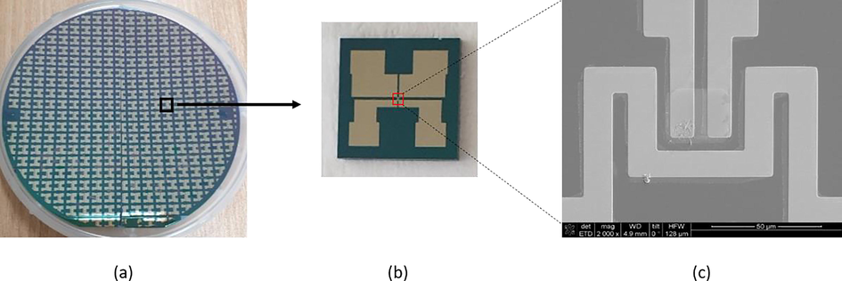
Photograph of the ZnO gas sensor of (a) 4-inch wafer, (b) one sensor, and (c) SEM image of Electrode and Heater patterns.
The present investigation focus on the ZnO nanorods gas sensors fabrication. The sensing material ZnO nanrods were synthesized by wet chemical method and hydrothermal method. The synthesized ZnO nanorods were systematically characterized by XRD, FTIR, XPS and SEM techniques. In sensor pattern, the Pt electrodes and heater were deposited in a pre-patterned using photolithography and lift off techniques. The sensing seed layer was deposited on a thin film by RF sputtering system. And there was studied about ZnO nanorods structures to improve sensor properties such as sensitivity, selectivity and response/recovery times.
2 Experimental details
2.1 Gas sensor component
The gas sensors typically consist of substrate, electrodes, heaters, and sensing materials. To simplify the process, two photomasks were used such as first for Pt/Ti deposition and second for the deposition of ZnO sensing materials. The photolithography and lift off techniques are used for the fabrication. The sensor photograph after completion of the device is shown in Fig. 1.
Silicon had an excellent oxide film (SiO2), abundantly exists on earth, stability as elemental semiconductor and ease of production, and excellent temperature characteristics have led to the dominance of semiconductor market. The SiO2 layer was used as thermal and electrical insulator. Temperature control is essential for gas sensors to work well. Because it has the optimum operating temperature according to sensing material. The two electrodes of the sensor play an important role in measuring the change of resistance when exposed to target gas. Platinum is used for heater and electrodes because of its high thermal and electrical stability at high temperature. In this work, a platinum heater and electrodes were designed on SiO2 layer like Fig. 1(c). That means electrode and heater patterns of one plane designs simply the process of sensor fabrication.
When the sensor is exposed to target gas, the sensing layer is a part where interacts with the gas on the sensor surface. At first, the ZnO seed layer was deposited by spin coater or RF sputtering device. Afterward the growth of ZnO nanorods carried out by chemical bath deposition and hydrothermal method.
2.2 Fabrication process
Fig. 2 (a-j) shows the fabrication processes of ZnO nanorods gas sensor. Fig. 2(a) shows a silicon wafer (4 in., 500 µm thickness, single sided polished, 〈1 0 0〉 oriented, p-type), which was sonicated with acetone for 10 min then washed with D.I. water and dried. To get 500 nm SiO2 layer, the Si wafer was oxidized by thermal oxidation as shown in Fig. 2 (b). Consequently, positive photoresist was deposited with 1.6 µm thickness by spin coating as shown in Fig. 2 (c) then pre-patterned electrodes and heater were deposited by using photolithography method in Fig. 2(d). Pt/Ti layer of 200 nm/10 nm thickness was deposited by DC sputtering system in Fig. 2(e). Titanium (Ti) and Platinum(Pt) layer means the adhesion and the electrodes and heater materials respectively. Then by using lift off method, pre-patterned electrodes and heater were obtained like Fig. 2 (f).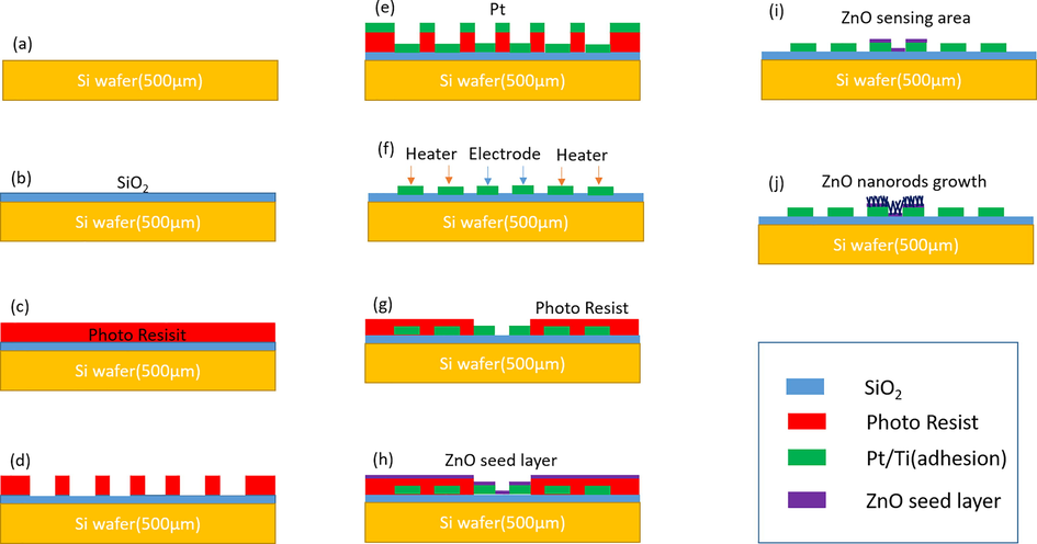
Fabrication processes of ZnO nanorods gas sensor; (a, b) Si wafer and thermal oxidized SiO2 layer, (c, d) deposition and pattern of photoresist, (e) Pt/Ti layer deposition, (f) electrode and heater pattern, (g) deposition and patterns of photoresist layer, (h) ZnO seed layer deposition, (i) ZnO sensing area and (j) ZnO nanorods growth.
Afterward, using second photomask which patterned sensing area, schemes of Fig. 2 (g) – (i) were carried out by photolithography and lift off techniques. ZnO seed layer of 30 nm thickness was deposited by RF sputtering system like Fig. 2 (i). Finally, vertical growth of ZnO nanorods was progressed selectively on ZnO seed layers by wet chemical process with a solution of zinc nitrate hexahydrate [Zn(NO3)2·6H2O] and hexamethylenetetramine [HMTA: C6H12N4] as shown in the Fig. 2(j). The solutions were made with mixing ratio 1:1 between Zn(NO3)2·6H2O and C6H12N4. The growth of ZnO nanorods was processed as below two types of wet chemical method namely, chemical bath deposition(CBD) method and hydrothermal(HD) method as shown in Fig. 3.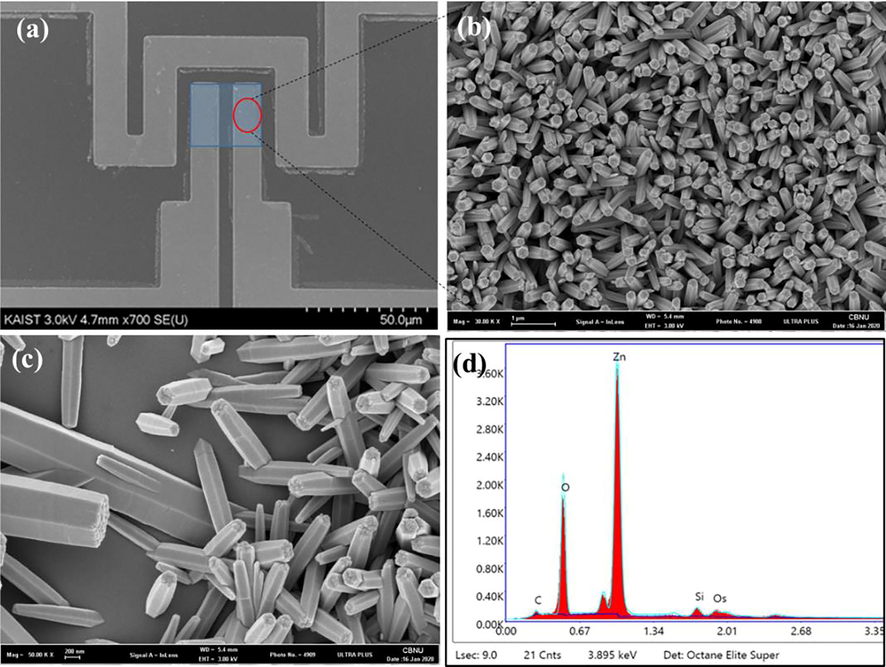
SEM images (Top-view) of vertically aligned ZnO nanorods in sensing area by chemical bath deposition (a-c) EDX spectra of ZnO nanorods (d).
2.3 Growth of ZnO nanorods by wet chemical method
Zinc acetate dehydrate((CH3COO)2Zn·2H2O), sodium hydroxide beads (NaOH), zincnitrate hexahydrate (Zn(NO3)2·6H2O), hexamethylenetetramine (C6H12N4) and ethyl alcohol(C2H5OH) were purchased from DAEJEUNG. All materials were used without any other treatments and purifications.
The chemical bath deposition (CBD) synthesis is to proceed the condensation and precipitation of the precursor solution compound on a substrate by dipping. Chemical reaction in bath results in precipitation on solid surface by saturation. Deposition thickness can be controlled by controlling the chemical reaction time. The CBD synthesis is used as growth of ZnO nanorods because of its merits such as low operating temperature, good compatibility with other devices and low cost (Li et al., 2010). The schematic diagram of ZnO nanorods synthesis process shown in Fig. SI. 1. Fig. SI. 1 (a) shows the schematic diagram of chemical bath deposition of ZnO nanorods. The pre-patterned ZnO seed layer substrate was dipped in freshly prepared growth solution at 80 °C for 1 h. Then the samples were taken out from the solution and thoroughly rinsed with DI water, and then dried in the oven at 80 °C for 4 h. In hydrothermal (HD) process, the growth solution and pre-patterned ZnO seed layer substrate was placed in the Teflon lined autoclave. Fig. SI. 1 (b) shows the schematic diagram of hydrothermal synthesis of ZnO nanrods. The hydrothermal method has some advantage such low cost, size controllability and reproducibility to make nanostructure. This method was done in an oven at 90 °C for 6 h. Next this sample was cleaned with DI water, and dried on the hot plate at 60 °C for 2 min. To obtain the stabilized material structure, annealing method was conducted for 5 h at 600 °C (Khoang et al., 2013).
2.4 Characteristic analysis
To analyze structural morphology and characteristics of sensing film, field emission scanning electron microscopy (FE-SEM, HITACHI SU8230) was used. The phase purity and crystallinity of synthesized ZnO nanorods were characterized by and X-ray diffraction (XRD, RIGAKU D/MAX-2500) and ATR-FTIR (Thermo Scientific USA). In addition, the chemical bonding was analyzed by X-ray & UV Photoelectron spectrometer (Thermo Scientific USA).
3 Results and discussions
3.1 Structural characteristic of ZnO nanorods
Fig. 3 shows SEM images and EDS spectra of grown ZnO nanorods by chemical bath deposition method. It can be seen that the ZnO nanorods with hexagonal top morphology uniformly grown at right angles on the pre-patterned electrodes. The average diameter of the formed ZnO nanorods are about 250 nm. Furthermore, the EDS spectra Fig. 4d confirmed the existence of the Zn and O elements.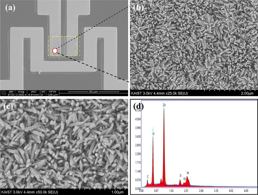
SEM images (Top-view) of vertically aligned ZnO nanorods in sensing area by hydrothermal deposition (a-c) EDX spectra of ZnO nanorods (d).
To explore the effect of synthesis route on the morphology and diameter of ZnO nanorods, the hydrothermally synthesized ZnO nanorods morphologies were analyzed by SEM and obtained results are shown in Fig. 4. The hydrothermally synthesized ZnO nanorods were uniformly grown on the patterned electrodes. The formed ZnO nanorods shown uniform length and diameter. The average diameter of the hydrothermally formed ZnO nanorods about 55 nm. The ZnO nanorods density increased in hydrothermal deposition than chemical bath deposition. In addition, the EDS spectra confirmed the presence of Zn and O elements in the nanorods.
The phase purity and crystalline structure of the synthesized ZnO nanorods were inspected by powder XRD. Fig. 5(a) shows the XRD pattern of ZnO nanorods. The XRD spectrum indicated the wrutzite hexagonal ZnO phase peaks with 2θ values of 31.77, 34.44, 36.26, 47.56, 56.60 and 62.89° belonging to the reflection of (1 0 0), (0 0 2), (1 0 1), (1 0 2), (1 1 0) and (1 0 3), respectively. The strongest peak (0 0 2) indicated growth along the c-axis of ZnO nanorods (Khoang et al., 2013, Li et al., 2010, Vanalakar et al., 2015, Wang et al., 2006). That is due to the fact that the (0 0 2) plane has the lowest surface energy with their c-axis perpendicular to the substrate, so it tends to grow fastest in that direction. In addition, the average crystallite size (D) of ZnO target material was calculated to be 55.02 nm using the first diffraction peak by Debye-Scherrer equation (Kadhim and Hassan, 2015)
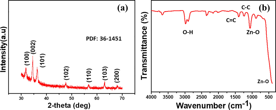
(a) XRD spectrum of ZnO nanorods (b) FTIR spectrum of ZnO nanorods.
Furthermore, the XPS pattern was obtained for ZnO nanorods and the XPS study results are shown in Fig. 6. The Fig. 6a shows the survey spectrum of the ZnO nanorods, confirmed the presence of Zn, O elements and trace amount of C in the sample. The deconvoluted Zn system (Fig. 6b) shows two major bonds Zn 2P 3/2 and Zn 2P ½ at binding energy 1021.4 eV and 1044.5 eV respectively. Which is well agreement with reported articles. The O1S spectrum (Fig. 6c) confirmed the ZnO, and C-O, C = O bonds at 530.6 eV and 532.7 eV respectively (Ramu et al., 2020). In addition, the XPS atomic percentage of ZnO nanrods shown in Fig. SI. 2. The obtained XPS results validate the FTIR results.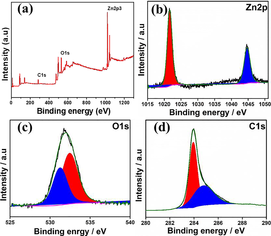
XPS spectrum (a) Survey spectrum (b) Zn 2P (c) O 1 s (d) C1s of ZnO nanorods.
3.2 Growth mechanism of ZnO nanorods
This mechanism is explained with chemical reaction of wet chemical process and theory of ZnO crystal nucleation and growth (Li et al., 2010, Wang et al., 2014). Zn(NO3)2·6H2O and C6H12N4 in growth solution provided Zn2+ and OH− ions, respectively. The chemical reactions of ZnO nucleation were progressed as follows (Li et al., 2010, Wang et al., 2014)
The polar surface of ZnO is so stable that it is easy to form various nanostructures. ZnO nanostructures followed the shape of wrutzite hexagonal ZnO structure. Fig. 7 shows scheme of growth mechanism of ZnO nanorods and ZnO structure. The top side and the bottom side are polar Zn2+ (0001) and polar O2− (000
), respectively. Typically, the morphology of ZnO crystals is explained by the growth velocity of each planes. According to [28], the fastest plane of growth was (0001) as followed
via hydrothermal process, which was corresponded with XRD result as shown in Fig. 5(a). Thus, ZnO nanorods were glowed along c-axis with direction (0001).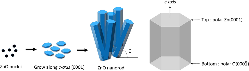
Scheme of growth mechanism of ZnO nanorods and ZnO structure.
3.3 ZnO nanorods interaction
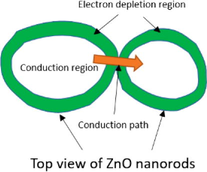
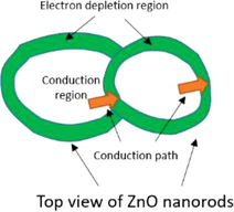
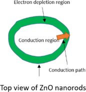
The well aligned ZnO nanorods have been focused to sense target gas for a long time (Khoang et al., 2013). The grown ZnO nanorods on patterned sensor electrodes were not all vertically aligned but some ones inclined or having junctions. When gas sensor based on ZnO nanorods is exposed to target gas, the electrical path or flow between nanorods decide the sensor performance. Overlapping of nanorods network was divided into three forms which are point, cross and block junctions (Khoang et al., 2013). Table 1 explains three junctions of ZnO nanorods overlapping via growth mechanism. First, the point junctions were denoted as meeting by a point between growing nanorods. After point contact, two nanorods grow in their own direction. Second, the cross junctions mean to cross between two nanorods. It is also to grow their own directions after crossing. Third, block junctions were denoted to block one nanorod growth by another nanorod. After crossing, it is possible just one nanorod growth. Among these junctions, the point junctions haven large change of the potential barriers before and after exposure to target gas have the most important effects on sensor (Khoang et al., 2013). Generally, electron flow is efficiently going on dense nanorods networks. However, the dense nanorods network sometimes interrupt the diffusion path of target gas into nanorods. So, the optimal growth conditions for well aligned nanorods should be requested because of contradicting as mentioned upper.
Junctions type
Diagram of junctions
Potential barriers
Diagram of grain boundaries
Growing process after junction
Point junction

Two direction maintain each other
Cross junction


Two direction maintain each other
Block junction

One nanorod is maintained own direction but another one is stopped
4 Conclusions
The ZnO nanorods gas sensor was successfully fabricated to detecting breath by wet chemical method (chemical bath deposition and hydrothermal method) with photolithography and lift off techniques. This ZnO gas sensor consisted of Si substrate, Pt electrodes and heater and ZnO sensing materials. The electrodes were used to sense the resistance when the gas sensor was exposed to target gases and the heater was used to make the optimum operating temperature for the sensing materials to work well. Also, the growth mechanism of ZnO nanorods was reported. According to XRD results, the (0 0 2) plane has the lowest surface energy with their c-axis perpendicular to the substrate, so it tends to grow fastest in that direction. The morphology of ZnO crystals is explained by the growth velocity of each planes. Thus, ZnO nanorods were glowed along c-axis with direction (0001). And the optimal morphology of grown nanorods for sensing target gas was discussed about three types junctions of nanorods overlapping such as point, cross and block junctions. The point junctions will have large change of the potential barriers before and after exposure to target gas have the most important effects on sensor. The control of experiment parameters such as growth time, growth temperature and seed layer should be considered sufficiently. Hence, the fabricated ZnO nanorod based gas sensor device is suitable for human breath analysis.
Acknowledgments
This research was supported by Nano · Material Technology Development program through the National Research Foundation of Korea (NRF) funded by the Ministry of Science, ICT and Future Planning. (2009-0082580). The authors extend their appreciation to Industry-academic cooperation Foundation New business R&D Program through the Small and Medium Venture Business Department. (S2779368). The authors extend their appreciation to the Researchers supporting project number (RSP- 2021/247) King Saud University, Riyadh, Saudi Arabia.
Declaration of Competing Interest
The authors declare that they have no known competing financial interests or personal relationships that could have appeared to influence the work reported in this paper.
References
- Adelyn, P. P., Hashim, U., Ha, Y. P., Arshad, M. M., Ruslinda, A. R., Ayub, R. M., Foo, K. L. 2015. Transparent mask design and fabrication of interdigitated electrodes. RSM2015 Proc., Kuala Terengganu, Malaysia (pp. 1-4). IEEE.
- Gas sensing properties of defect-controlled ZnO-nanowire gas sensor. Appl. Phys. Lett.. 2008;93(26):263103
- [Google Scholar]
- Phosphorus acceptor doped ZnO nanowires prepared by pulsed-laser deposition. Nanotechnology. 2007;18(45):455707
- [Google Scholar]
- α-Fe2O3 nanotubes in gas sensor and lithium-ion battery applications. Adv. Mater.. 2005;17(5):582-586.
- [Google Scholar]
- Raman scattering and efficient UV photoluminescence from well-aligned ZnO nanowires epitaxially grown on GaN buffer layer. J. Phys. Chem. B. 2005;109(18):8749-8754.
- [Google Scholar]
- Effect of Ni doping on thick film SnO2 gas sensor. Sens. Actuators B Chem.. 2006;113(2):823-829.
- [Google Scholar]
- Jayaraman, T., Murthy, A. P., Lee, S. J., Karuppasamy, K., Arumugam, S. R., Yu, Y., Choi, M. Y. 2020. Recent progress on synthetic strategies and applications of transition metal phosphides in energy storage and conversion. Ceram. Int.
- Rapid and selective detection of acetone using hierarchical ZnO gas sensor for hazardous odor markers application. J. Hazard. Mater.. 2014;276:262-270.
- [Google Scholar]
- Effects of glycerin volume ratios and annealing temperature on the characteristics of nanocrystalline tin dioxide thin films. J. Mater. Sci. Mater. Electron.. 2015;26(6):3417-3426.
- [Google Scholar]
- TiO2 thin film gas sensor for monitoring ammonia. Mater Charact. 2007;58(8–9):680-684.
- [Google Scholar]
- Karuppasamy, K., Rabani, I., Vikraman, D., Bathula, C., Theerthagiri, J., Bose, R., Kim, H. S. 2020. ZIF-8 templated assembly of La3+-anchored ZnO distorted nano-hexagons as an efficient active photocatalyst for the detoxification of rhodamine B in water. Environ. Pollut., 116018.
- Comparative study of the cytotoxic and genotoxic potentials of zinc oxide and titanium dioxide nanoparticles. Toxicol. Rep.. 2015;2:765-774.
- [Google Scholar]
- On-chip growth of wafer-scale planar-type ZnO nanorod sensors for effective detection of CO gas. Sens. Actuators B Chem.. 2013;181:529-536.
- [Google Scholar]
- Synthesis of ZnO nanorod on bare Si substrate using metal organic chemical vapor deposition. Physica B Condens. Matter. 2003;328(3–4):368-371.
- [Google Scholar]
- Controlled selective growth of ZnO nanorod and microrod arrays on Si substrates by a wet chemical method. Appl. Phys. Lett.. 2006;89(16):163128
- [Google Scholar]
- Single-crystal nanorings formed by epitaxial self-coiling of polar nanobelts. Science. 2004;303(5662):1348-1351.
- [Google Scholar]
- Different origins of visible luminescence in ZnO nanostructures fabricated by the chemical and evaporation methods. Appl. Phys. Lett.. 2004;85(9):1601-1603.
- [Google Scholar]
- Controllable growth of well-aligned ZnO nanorod arrays by low-temperature wet chemical bath deposition method. Appl. Surf. Sci.. 2010;256(6):1698-1702.
- [Google Scholar]
- Highly sensitive WO3 hollow-sphere gas sensors. Inor. Chem.. 2004;43(17):5442-5449.
- [Google Scholar]
- Ordered semiconductor ZnO nanowire arrays and their photoluminescence properties. Appl. Phys. Lett.. 2000;76(15):2011-2013.
- [Google Scholar]
- Gas-sensing properties of well-crystalline ZnO nanorods grown by a simple route. Physica E Low Dimens. Syst. Nanostruct.. 2007;36(1):102-105.
- [Google Scholar]
- TiO2-based gas sensor: a possible application to SO2. ACS Appl. Mater. Interfaces. 2013;5(17):8516-8522.
- [Google Scholar]
- Synthesis of hierarchically structured T-ZnO-rGO-PEI composite and their catalytic removal of colour and colourless phenolic compounds. Chemosphere. 2020;129245
- [Google Scholar]
- Sensitive and selective NO2 gas sensor based on WO3 nanoplates. Sens. Actuators B Chem.. 2017;240:426-433.
- [Google Scholar]
- Recent advances in 2-D nanostructured metal nitrides, carbides, and phosphides electrodes for electrochemical supercapacitors–A brief review. J Ind Eng Chem. 2018;67:12-27.
- [Google Scholar]
- Recent advances in metal chalcogenides (MX; X= S, Se) nanostructures for electrochemical supercapacitor applications: a brief review. Nanomaterials. 2018;8(4):256.
- [CrossRef] [Google Scholar]
- Optical and electrical properties of ZnO nanowires grown on aluminium foil by non-catalytic thermal evaporation. Nanotechnology. 2007;18(17):175606
- [Google Scholar]
- Controlled growth of ZnO nanorod arrays via wet chemical route for NO2 gas sensor applications. Sens. Actuators B Chem.. 2015;221:1195-1201.
- [Google Scholar]
- Fabrication of a SnO2 nanowire gas sensor and sensor performance for hydrogen. J. Phys. Chem. C. 2008;112(17):6643-6647.
- [Google Scholar]
- Hydrothermally grown oriented ZnO nanorod arrays for gas sensing applications. Nanotechnology. 2006;17(19):4995.
- [Google Scholar]
- Alignment-controlled hydrothermal growth of well-aligned ZnO nanorod arrays. J Phys Chem Solids. 2014;75(7):808-817.
- [Google Scholar]
- Induced growth of asymmetric nanocantilever arrays on polar surfaces. Phys. Rev. Lett.. 2003;91(18):185502
- [Google Scholar]
- ZnO Nanofiber Field-Effect Transistor Assembled by Electrospinning. Ceram. Soc.. 2008;91(2):656-659.
- [Google Scholar]
- Low-temperature growth of well-aligned ZnO nanorods by chemical vapor deposition. Adv. Mater.. 2002;14(3):215-218.
- [Google Scholar]
- Preparation of ZnO nanorods through wet chemical method. Mater. Lett.. 2007;61(30):5202-5205.
- [Google Scholar]
- An acetone gas sensor based on nanosized Pt-loaded Fe2O3 nanocubes. Sens. Actuators B Chem.. 2019;290:59-67.
- [Google Scholar]
- Synthesis and luminescence properties of ZnO: Tb3+ nanotube arrays via electrodeposited method. Physica B Condens. Matter. 2010;405(15):3200-3204.
- [Google Scholar]
- Room-temperature gas sensing of ZnO-based gas sensor: A review. Actuator A Phys.. 2017;267:242-261.
- [Google Scholar]
Appendix A
Supplementary data
Supplementary data to this article can be found online at https://doi.org/10.1016/j.jksus.2021.101397.
Appendix A
Supplementary data
The following are the Supplementary data to this article: