

Fabrication of high voltage gradient ZnO nanoparticle-Bi2O3-Mn2O3-based thick film varistors at various sintering temperature
-
Received: ,
Accepted: ,
This article was originally published by Elsevier and was migrated to Scientific Scholar after the change of Publisher.
Peer review under responsibility of King Saud University.
Abstract
In this research, 20 nm zinc oxide nanoparticles were utilized to fabricate significant voltage gradient zinc oxide nanoparticle-Bi2O3-Mn2O3-based thick film varistors (TFVs) by applying screen printing method. Different low temperatures during the sintering process had a considerable effect on the zinc oxide nanoparticle-based TFVs. In particular, the low temperatures improved the growth of ZnO grains, which was obvious even at 550 °C. The huge surface area of the 20 nm zinc oxide encouraged an intense surface interaction even at minimal sintering temperatures. The sintering technique also enhanced the internal structure of the crystal. Minimizing the fundamental compressive stress depended on the XRD lattice constant and the FWHM analysis. The variable temperatures of the sintering process considerably impacted the electrical behaviours of the samples. A remarkable increase in the voltage gradient of the varistor sintered up to 5732.5 V/mm at 700 °C was observed. The electrical resistivity dropped dramatically from 621.8 kΩ.cm (varistor at 550 °C) to 147.3 kΩ.cm at 800 °C sintering temperature. The small size of grains with perfect boundaries was the main reason for the enhancement of the voltage gradient. The optimal electrical characteristics with a 63 nonlinearity coefficient and 103 μA leakage current were achieved in the varistor sintered at 700 °C. Moreover, maximum permittivity and minimum dissipation factor were attained through the minimal frequency range. Therefore, the sintering process could be applied as a novel technical approach for the dominant voltage gradient of zinc oxide nanoparticle-based TFVs with enhanced microstructural and electrical behavior and good nonlinearity.
Keywords
ZnO nanoparticles
Sintering
Thick film varistor
Growth
Voltage gradient

1 Introduction
Electrical and electronic techniques, such as a surge protection system, have been applied to the varistor system for many years due to optimal nonlinearity exponent and minimal leakage current. Several electrical parameters, such as break down voltage and resistivity value of these systems, rely significantly on structural status; consequently, the grain size and structural uniformity are among the factors with the greatest influence in a varistor fabrication technique (Takada and Yoshikado, 2010).
Significant requirements exist for varistors existence miniature and combination with huge voltage gradient (Chen et al., 2017). Commercial zinc oxide varistors are ceramic discs that are unable to meet the requirements for certain implementations, such as a varistors array, surface applied techniques, and others. Considering the fact that they are huge products with minimum value and ingenuous design, zinc oxide-based thick film varistors (TFVs) are fabricated to become appropriate exchanges and to obtain the general interest (Debeda-Hickel et al., 2005; Jadhav et al., 2016; Paun, 2017).
There are many techniques (Jadhav et al., 2016; Paun, 2017; Al Abdullah et al., 2017; De La Rubia, 2017; de la Rubia et al., 2004) used to prepare zinc oxide-based TFVs; these techniques include sol–gel technique, screen printing, direct-writing technique, and so on. Khalaf et al. (Al Abdullah et al., 2017) fabricated TFVs via a sol–gel technique using 200 μm film thickness at 1000 °C sintering temperature. Paun et al. (Paun, 2017) obtained zinc oxide-based TFVs via direct write method using Na dopant with 1200 V/mm voltage gradient; they clarified that zinc oxide-based TFVs can be sintered at 900 °C. Rubia et al. (De La Rubia, 2017) prepared the zinc oxide-based TFVs with a huge voltage gradient rate of approximately 2000 V/mm via tape casting technique at 950 °C sintering temperature.
However, investigating the industrialization of the intended target using these methods is still very complicated due to the high cost and complicated experiment processes. Jadhav et al. (Jadhav et al., 2016) fabricated zinc oxide-based TFVs via screen printing at 900 V/mm voltage gradient at 1150 °C sintering temperature. Rubia et al. (de la Rubia et al., 2004) suggested a technique to enhance the voltage gradient via the substitution of Bi2O3 and Sb2O3 with the Bi38ZnO58 sillenite phase and Zn7Sb2O12 orthorhombic spinel phase, respectively. They applied the screen printing technique at 900 °C sintering temperature at 1000 V/mm voltage gradient. However, using the devices on a significant voltage area by these two methods is intractable despite the benefits of lower costs and ease of the process (via screen printing) because of the low voltage gradient caused by the sintering process at very high temperature.
In many previous studies (Chen et al., 2017; De La Rubia, 2017; Kim and Kim, 2021; Kazani, 2012); ZnO-based TFVs samples were sintered at temperatures higher than 850 °C, which caused a significant increase in the size of ZnO grain after the annealing process, leading to the reduction of the grain boundary and large volatilization of Bi2O3 at high temperature, which in turn decreased the voltage gradient and led to deterioration of boundary insufficiency among the grains; the linear properties did not appear to cause the absence of nonlinearity behaviors (Sim et al., 2018; Kamrani et al., 2018). In the current research, significant voltage gradient zinc oxide-based TFVs were manufactured by applying screen printing method and substituting the traditional zinc oxide microparticle powder with zinc oxide nanoparticle powder (20 nm), which has superior sintering ability; such TFVs had many remarkable characteristics due to several surface properties and nanoparticle morphology, which contributed to the reduction of the temperature during the sintering process. Furthermore, this study investigated whether sintering temperature impacts crystallite, electrical, and dielectrical characteristics of TFVs fabricated from zinc oxide nanoparticle powder.
2 Experimental details
2.1 Sample preparation
The raw materials applied in this work were of significant purity and quality. Below are the raw materials list and their corresponding properties. The technical specifications of the raw materials are posted in following Table.
| Material | Chemical formula | Purity (%) | Mean size | Supplier |
|---|---|---|---|---|
| Nanoparticles Zinc Oxide | ZnO | > 99.9 | 20 nm | MKNANO Canada |
| Bismuth Trioxide | Bi2O3 | > 99.9 | 10 µm | SEGMA-ALDAICH |
| Manganese Trioxide | Mn2O3 | > 99.9 | 0.7 µm | SEGMA-ALDAICH |
The powder was blended with poly vinyl alcohol (PVA) by mixing with distilled water in a ball milling jar for 6 h. The ZnO slurry was dried at 60 ± 5 °C in air for 1 h and then granulated by sieving through a 20-mesh sieve. The thick film pastes for screen printing were formed as follows: 60% in weight of active powder was homogenized and mixed for 30 min with 40% in weight of an organic vehicle, which composed of α-terpineol as the solvent, ethylcellulose as the binder, and [2-(2-butoxi-etoxi-ethyl)] acetate as plastificant. Dolapix was used as a dispersant. Before the deposition of ZnO-based varistor pastes onto dense alumina substrates, commercial silver paste electrode was screen printed onto the substrates and fired at 800 ± 0.5 °C for 1 h. Afterward, layers of varistor ink were deposited by screen printing by a DEK 65 screen printing machine with a polyester mesh. Each layer was dried in an oven at 120 ± 0.5 °C for 15 min. Each green layer had a thickness of around 10 μm (±0.3–0.5%). When>10 layers were deposited, structural defects appeared after drying. Therefore, the highest green thickness that can be obtained for this paste is around 100 μm. To avoid the appearance of cracks, six layers of varistor paste were deposited. For all the films, green thickness was in the range of 60–70 μm (±0.2–0.5%), in accordance with the mesh opening and the number of deposited layers. Finally, the green samples were sintered at 550 °C, 600 °C, 650 °C, 700 °C, 750 °C, and 800 °C in air with 1 h soaking time.
2.2 Characterization
The crystalline phases of ZnO-based thick film varistor were identified through powder X-ray diffraction (XRD, Diano XRD-8545, λCu Kα radiation).
The microstructure of ZnO-based TFVs was studied using a scanning electron microscopy (SEM) system (model: JSM – 6460 LV). Grain size was estimated from SEM images via the linear intercept method (Campus, 2013; Kharchouche, 2018; Wurst and Nelson, 1972).
The density of the samples after the sintering process was determined (Gheisari et al., 2020) using the SEM images by estimating the ZnO grain and empty area ratio and subsequently converting the area ratio (Rarea) to the coinciding volumetric ratio (Rvolume =
2.3 Electrical testing
The electrical behaviors of ZnO-based thick film varistor were obtained by applying a high voltage source unit (KEITHLEY system 246). The breakdown voltage (Vb) was calculated at 1.0 mA/cm2 current density and the voltage gradient (E1mA) was calculated via E1mA = Vb/d, whereas d is the varistor thickness. The leakage current (IL) was investigated at 0.75 ± 0.05 Vb electrical field and the nonlinearity value (α) was specified between 1.0 and 10 ± 0.5 mA/cm2 in current density. The dielectric parameters in ZnO-based thick film varistor (TFVs), involving the permittivity (εr) and the dissipation factor (tan δ) were obtained applying a precision impedance analyzer.
3 Results and discussion
3.1 Microstructural analysis
3.1.1 Scanning electron microscopy
Fig. 1 presents the SEM images of 20 nm zinc oxide-based thick film varistor at difference temperatures during the sintering process. These images indicated that the morphology of the varistors surface was significantly affected by the sintering temperature, and the density and size of grains in the TFVs were increased at the highest temperature of 800 °C. The grains’ sizes increased to about 1.2, 1.5, 2.3, 2.9, 3.4, and 4.1 μm with increasing sintering temperatures (550 °C, 600 °C, 650 °C, 700 °C, 750 °C, and 800 °C, respectively), as shown in Table 1.
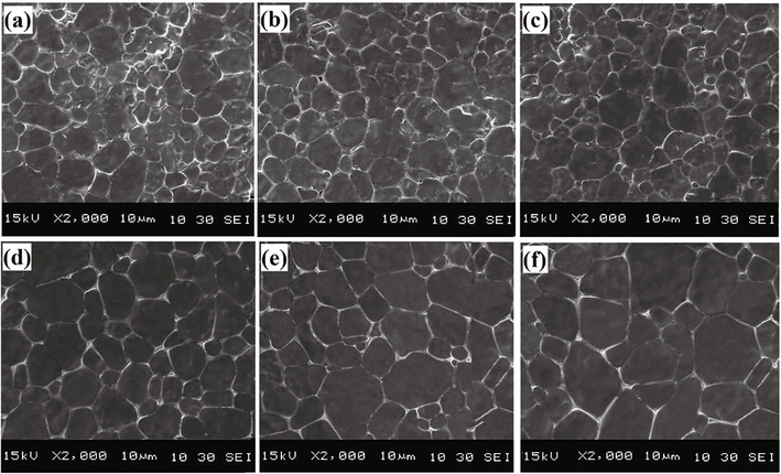
- Typical SEM micrographs of ZnO nanoparticles-Bi2O3-Mn2O3-based thick film varistors ceramics sintered at (a) 550 °C, (b) 600 °C, (c) 650 °C, (d) 700 °C, (e) 750 °C, and (f) 800 °C temperatures.
| Sintering temperature | Density g/cm3 | SEM | XRD | |||
|---|---|---|---|---|---|---|
| Grain size (μm) | 2θ (deg.) | A (Å) | C (Å) | Stress (σ) (G.Pa) | ||
| 550 °C | 64 | 1.2 | 36.13 | 3.240 | 5.221 | −1.306 |
| 600 °C | 69 | 1.5 | 36.17 | 3.237 | 5.214 | −0.699 |
| 650 °C | 73 | 2.3 | 36.20 | 3.234 | 5.211 | −0.435 |
| 700 °C | 77 | 2.9 | 36.24 | 3.228 | 5.205 | 0.086 |
| 750 °C | 79 | 3.4 | 36.27 | 3.224 | 5.202 | 0.349 |
| 800 °C | 86 | 4.1 | 36.29 | 3.219 | 5.189 | 1.483 |
The porosity of ZnO grains diminished, and their sizes grew obviously until they resembled regular polygons or hexagons. High temperatures during the sintering process provided a greater driving force for interior crystalline diffusion, leading to the significant growth of ZnO grains and pore reduction. The considerable sample densification at high sintering temperatures may have been caused by the added impact of Bi2O3 and the Mn2O3 within the zinc oxide crystal, which led to the production of O2 vacancies through the sintering technique. When the doping ions were replaced at the zinc ion site through the sintering step, oxygen vacancies were formed and participated in the improvement of the sintered samples’ density. All the samples presented a porous microstructure. The estimated values of sample density were 64, 69, 73, 77, 79, and 86 vol% at the sintering temperatures of 550 °C, 600 °C, 650 °C, 700 °C, 750 °C, and 800 °C, respectively. These values of the samples’ densities obtained from the SEM micrographs can possibly be used to compare the film densities but cannot be considered as absolute values.
A motivating observation was the obvious existence of several spinel and liquid phases in the samples sintered at temperatures above 650 °C. Such phases may prevent the grains’ growth through the sintering technique. These mentioned phases ordinarily exist in groups or separated and are sometimes inside the zinc oxide grains. The liquid phase during sintering produced Bi-rich phases, which were associated with the spinel particles in the intergranular region of the microstructure.
The obvious existence of Bi was clear at the zinc oxide grain boundary (GB) among the ZnO grains for the samples sintered at the temperatures above 650 °C. The disappearance of bismuth in these samples may be attributed to the fact that the boundaries in the varistor at low sintering temperatures were not consistent. Considerable amounts of Bi ions with huge ionic sizes were obviously separated to the grain boundaries. These ions were exposed to obstacles occupying interstitial sites within the zinc oxide grains attributed to further donor occupation. The ions stabilized within the grain boundaries to the composed Bi-rich phases because of the ions’ inability to squeeze inside the crystal atoms due to the significant sizes of the grains. The phases of Bi-rich among the grain boundaries play a significant role in oxygen transport to the zinc oxide grains through the sintering technique (Liu et al., 2013; Tahmasebi et al., 2018; Xu et al., 2016; Akinnifesi et al., 2014). Nevertheless, the generality of the boundaries among the grains included a continual intergranule Bi-rich element at considerable Bi2O3 concentrations, as revealed in the varistors after the sintering process, due to the Bi2O3 liquid phase. Such phenomenon was attributed to pyrochlore disintegration during significant temperatures, thereby wetting the zinc grains and subsequently freezing them at normal temperature (Metz et al., 2000).
3.1.2 X-ray diffraction
Fig. 2 displays the X-ray diffraction analysis of the zinc oxide nanoparticle-based thick film varistor system distinguished via the highest main spectra of (1 0 0), (1 1 0), (1 0 1), and (0 0 2), which originated from the zinc oxide grains (JCPDS Card No. 36–1451) and were emphasized by the multicrystalline kind of samples. Other spectra also appeared as secondary phases and were called the α-Bi2O3 (JCPDS Card No. 27–0050), Bi48ZnO73 (JCPDS Card No. 41–1449) and Mn3O4 phases (JCPDS Card No. 24–0734). These materials contained zinc oxide and are known as a superior phase. Liquid, spinal, pyrochlore, and various secondary phases existed in the samples, except for samples sintered at 550 °C and 600 °C. A previous sintering study (Huang et al., 2013) reported that the consistency of these spectra within a varistor system required temperatures above 600 °C. The formation of secondary phases was related to the concentration of dopants to the varistor and the procedure conditions. The integration of different oxides constructs crystal imperfections at the ZnO grain and boundaries among the grains (Liu, 2019; Masteghin et al., 2017).
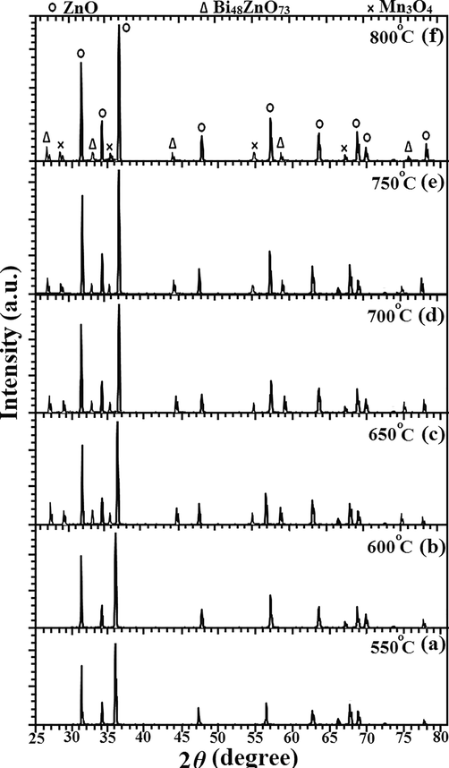
- XRD patterns of ZnO nanoparticles-Bi2O3-Mn2O3-based thick film varistors ceramics sintered at (a) 550 °C, (b) 600 °C, (c) 650 °C, (d) 700 °C, (e) 750 °C, and (f) 800 °C temperatures.
The increase in the temperature through the sintering process caused maximum and narrower peaks and minimum FWHM for the varistor, demonstrating the sample’s superior crystalline and structural arrangement, which was obtained in the varistor at 800 °C (Fig. 2(f)) and through the minimal peak intensity of the varistor at 550 °C (Fig. 2(a)).
The height of the (1 0 1) peak incremented from 2θ = 36.13° to 2θ = 36.17° in the sample sintered at 600 °C, revealed the appearance of residual stress within the zinc oxide nanoparticle-based TFV. Increasing the sintering temperatures leads to the narrowing of the (1 0 1) peak, a lower unsymmetrical, and a gradual change to upper 2θ values, thereby causing the reduction in the lattice constant (Table 1). Furthermore, the FWHM value of the (1 0 1) line decreased with increasing temperature of the sintering process (Table 1), indicating that the sintering technique enhanced the crystallinity of the 20 nm zinc oxide. The FWHM values of the (Bi48ZnO73) and (Mn3O4) developed with increasing temperature, and the diffraction peak intensity weakened. The peak intensities of these phases for the varistor sintered at 800 °C were obviously less compared with those sintered at 650 °C, 700 °C, and 750 °C due to the limited evaporation of Bi2O3. The loss of Bi2O3 phase within the varistor sintered at 800 °C unavoidably led to the nonlinear diminishing.
Through the growth procedure, the compressive stress compound value was greater than the thermal (tensile) stress compound value. Consequently, the sample sintered at 650 °C demonstrated a comprehensive compressive residual stress (Wang, 2016). With increasing sintering temperature, the compressive stress transformed to tensile stress.
Table 1 presents the SEM and XRD analysis results. Based on the following Equation (1), the lattice constant “c” was obtained as follows (Alvarez et al., 2016):
where h, k, and l were estimated using the XRD information. The atomic spacing d was obtained from the Bragg's equation (Alvarez et al., 2016):
The lattice constant (c) of the zinc oxide nanoparticle-based TFV varistor was evaluated based on the situation of (0 0 2) phase in the ZnO crystal in Table 1. These lattice constant (c) values are identical to the bulk ZnO lattice constants c0 at 5.206 Å (Alvarez et al., 2016). Utilizing the above data, the stress (σ) within the sample was obtained by applying the strain model as follows (Wang et al., 2015; Zhi et al., 2003):
whereas σ is the average stress within the varistor, C11 = 209.7 GPa, C12 = 121.1 GPa, C13 = 105.1 GPa, and C33 = 210.9 GPa are the elastic stiffness constants of bulk ZnO (-453.6 GPa). The calculated stress “σ” values within the varistor for (0 0 2) plane developed at various low sintering temperatures are listed in Table 1. The increase in the stress order values was as follows: σ(a) < σ(b) < σ(c) < σ(d) < σ(e) < σ(f). The negative compressive stress values suggested that the lattice constant was extended compared with the stress-free varistor (Wang et al., 2015). The varistors sintered at 700 °C, 750 °C, and 800 °C exhibited a positive value, which suggested that the tensile stress resulted from the expansion size of lattice, thereby revealing that the lattice constant was less elongated than in the stress-free sample.
3.2 Electrical properties
3.2.1 V-I Behavior
Fig. 3(a) presents the V-I characteristics (in E-J indication) of the ZnO nanoparticle-based TFV at various temperatures during the sintering process. The electric current was used, and the continuous voltage was predestined. The E-J relations in Fig. 3(a) were like a diode feature with a linear and nonlinear zone. The nonlinear area revealed a low resistivity zone, whereas the nonlinear coefficient (α) was calculated from the following equation (Adl et al., 2015):
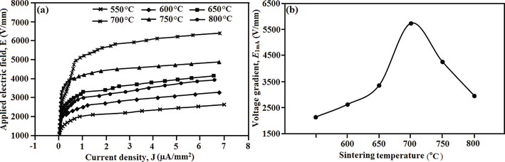
- (a) E-J characteristic of ZnO nanoparticles-Bi2O3-Mn2O3-based thick film varistors at different sintering temperatures, and (b) variation of the voltage gradient as a function of the different sintering temperatures.
The E-J curve indicated that the elbow of curves among the minimum electric field region before breakdown voltage and maximum electric field region at breakdown region was responsible for a considerable function in the electrical behavior of ZnO nanoparticle-based TFVs. The sharper elbow indicated the optimal nonlinear characteristic. Varistors at 650 °C, 700 °C, and 750 °C sintering temperatures exhibited almost identical forms of conduct curves and showed superior nonlinear behaviors. However, the varistors at 550 °C, 600 °C, and 800 °C sintering temperatures showed the poor nonlinearity by presenting an almost rounded elbow.
Table 2 presents the various parameters of the electrical characteristics of ZnO nanoparticle-based TFVs specimens involving the voltage gradient (E1mA), withstanding voltage (Vb), resistivity (ρ), nonlinear constant (α), barrier height (ΦB), density of interface states (NIS), width of depletion layer (ω), and donor density (Nd). ΦB and ω were investigated from the thermionic emission theory (Cortés et al., 2018), which is lnJ = β½/kT + lnA*T2 - ΦB/kT, where β α 1/ω is obtained from the depletion layer width, and A* is known as Richardson‘s constant. NIS and Nd are calculated from the equations NIS = Nd/ω and Nd = 2εΦB /e2ω2.
| Sintering temperature | E1MA (V/mm) | Vb (V) | α | Ρ (kΩ.cm) | IL (µA) | Nd (m3) (x1024) | NIS (m−2) (x1016) | ФB (eV) | ω (nm) |
|---|---|---|---|---|---|---|---|---|---|
| 550 °C | 2140.8 | 2.57 | 40 | 621.8 | 613 | 1.3 | 1.4 | 0.4 | 56.4 |
| 600 °C | 2622.5 | 3.93 | 48 | 487.2 | 588 | 2.6 | 3.5 | 1.5 | 45.8 |
| 650 °C | 3352.2 | 7.71 | 57 | 339.4 | 229 | 4.8 | 4.9 | 2.2 | 33.6 |
| 700 °C | 5732.5 | 16.6 | 63 | 266.4 | 103 | 7.3 | 7.8 | 4.3 | 19.9 |
| 750 °C | 4260.3 | 14.5 | 12 | 218.5 | 276 | 2.1 | 3.9 | 2.9 | 39.4 |
| 800 °C | 2963.6 | 12.2 | 8 | 147.3 | 393 | 0.9 | 2.2 | 1.7 | 53.8 |
The lower of the breakdown voltage value (Vb) of the sample sintered at 550 °C may have been caused by the minimal boundaries among the ZnO grains and decreased “p-n junctions.” Less “p-n junctions” produced minimum breakdown voltages. The value of average breakdown voltage across single grain/grain boundary can be calculated by the following equation: Vb = E1mA D.
The addition of Bi2O3 to the varistor led to the maximum nonlinear value (α). Therefore, Bi2O3 showed a considerable impact on the boundaries’ Schottky barrier within the ZnO nanoparticle-based TFVs. The loss of Bi2O3 at very high sintering temperature is related to minimum, and broad barrier leads to the electronic idle of boundaries and degenerates the nonlinearity behaviors. Moreover, Mn2O3 is generally added to a sample as a dopant to construct the Schottky barrier within the boundaries. At a significant temperature of sintering process, Mn is demonstrated as a deep donor within the varistor and reduces the intrinsic donor concentration ([31]; Roy et al., 2016; Zhou et al., 2004). Mn addition exhibited a considerable impact on the boundary compared with the effect on the ZnO grain, referring to the fact that the boundaries among the grains were more highly resistive compared with the zinc grains.
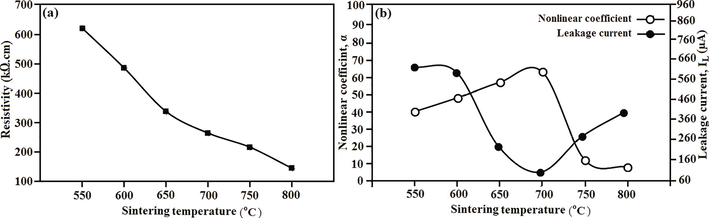
Figs. 3, 4, and 5 show the parameters of electrical behavior in ZnO nanoparticle-based TFVs at different temperatures during the sintering process. As shown in Fig. 3(b), the E1mA value substantially followed the sintering temperature. With increasing sintering temperature, the value of E1mA increased gradually. With further increase in temperature, the E1mA value decreased dramatically. The E1mA reached the maximum value of 5732.5 V/mm for the varistor at 700 °C during the sintering process, and then, the value decreased for the samples sintered at 750 °C and 800 °C. However, all sintered samples presented a significant voltage gradient value, which exceeded 2000 V/mm. The electrical resistivity (ρ) for the sample sintered at 800 °C dropped significantly from 147.3 kΩ.cm to 621.8 kΩ.cm for the sample sintered at 550 °C as presented in Fig. 4(a). Therefore, the sample sintered at 800 °C exhibited a reduction in potential barrier within the “p-n junctions,” leading to significant deterioration in ρ. Fig. 4(b) exhibits the variation of α and IL with different temperatures during the sintering process. Generally, the deviation of IL with various temperature was inverse to that of α. The IL exhibited the lowest value (103 μA), and α presented the upper value (63) for the samples sintered at 700 °C. The effects of sintering temperatures on IL and α are identical to their effects on E1mA. Varistors achieved optimum E1mA, IL, and α values at 700 °C sintering temperature. However, increasing the sintering temperature to more than this range led to the abrupt decrease in the E1mA and α value and acute increase in the IL value. Thus, the electrical behavior of zinc oxide nanoparticle-based thick film samples was significantly influenced by the increment of sintering temperature. The deterioration of E1mA and ρ, as well as IL and α, was observed when the sintering temperature exceeded 700 °C.
-
Variation of (a) resistivity, and (b) nonlinear coefficient and leakage current of ZnO nanoparticles-Bi2O3-Mn2O3-based thick film varistors with different sintering temperatures.
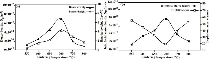
- The C–V behavior parameters including: (a) donor densities and barrier heights, and (b) interfacial states density and depletion layer of ZnO nanoparticles-Bi2O3-Mn2O3-based thick film sintered at different temperatures.
Furthermore, the Nd, NIS, and ΦB show the same behaviour as E1mA values. The ω has an inverse relationship with E1mA. The ΦB increases to a superior value of about 4.3 eV at 700 °C, but minimizes to 1.7 eV with increasing temperature up to 800 °C. The value of ω reduced from 56.4 eV to 19.9 eV for the samples sintered at 550 °C and 700 °C, but these values increased with increasing temperature during the sintering process. The variations of ΦB and ω with diverse temperatures may be due to the Schottky barrier composition within the boundary of ZnO grains. Huge and narrow barriers in the sample sintered at 700 °C played an essential role in improving the electrical characteristics of ZnO nanoparticle-based TFVs, especially in terms of E1mA, ρ, and α.
3.2.2 Dielectric properties
Fig. 6 shows the difference of the dielectric parameters with the frequency for ZnO nanoparticle-based TFVs at various temperatures of the sintering process. Fig. 6(a) shows that the varistor at 700 °C sintering temperature presented the optimum permittivity (εr) during the mensuration frequency range. The εr exhibited elevated values with increasing frequency value from 102 Hz to 105 Hz. However, with increasing frequency, the value of εr deteriorated significantly to 105 Hz. At the minimum frequency range, the efficient capacitance of the varistor resulted from the boundaries of the grains, and the elevated εr value within this range showed that the boundaries among the ZnO grains formed at 700 °C were better. Otherwise, the sharp drop in the εr at the elevated frequency area could be due to the polarization created within the narrow boundaries among ZnO grains. The capacitance of the grain had a significant function in εr during further frequency augmentation. Increasing the sintering temperature led to the initial increment of the εr value, which subsequently minimized due to the grain boundary layer capacitance (GBLC) impact (Nithya and Kalyanasundharam, 2019; Wu et al., 2002). In consonance with the GBLC impact, the εr of ZnO nanoparticle-based TFVs may be estimated as εr = ε (D/ω), where D is the mean size of ZnO grain, ω is the depletion layer width, and ε is the permittivity of ZnO. This equation elucidated that εr was controlled by the ZnO grains size and the thin insulative layer, which demonstrated the proportional relation to the size of ZnO grains and the inverse relation to the depletion of layer width. During the sintering process, the thickness of the depletion layer had a considerable impact on εr value in comparison with the slow development in the size of grains. The mean size of grains and depletion layer thickness increased at high sintering temperature (over 700 °C), thereby reducing the εr value. Fig. 6(b) demonstrated that the dissipation factor (tanδ) considerably depended on the temperature during the sintering process. The TFVs exhibited distinctly dispersion with the rising frequency between 102 and 104 Hz, and the varistor with 700 °C sintering temperature had the minimal tanδ value. The value of dielectric loss was specified via the boundary resistance and relied on electric conductance property during the depressed frequency field (Maleki Shahraki et al., 2019). Minimal value of tanδ during sintering in 700 °C proposed that the boundaries among the grains constructed within the varistor at this sintering temperature were superior to the others constructed at other sintering temperatures. Moreover, in Fig. 6(b), the peak of dielectric loss in all varistors was prominent at ∼ 105 Hz and was considerably affected by polarization loss during this critical frequency field. Credson et al. (de Salles et al., 2016) believed that the dielectric loss peak is attributed to thermion polarization. The manufacturing conditions and substance composition had respectable effects on the dielectric loss peak (de Salles et al., 2016).
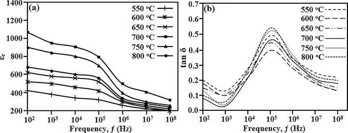
- Dielectric properties of ZnO nanoparticles-Bi2O3-Mn2O3-based thick film sintered at different temperatures; (a) εr – ƒ, and (b) tanδ – ƒ.
4 Conclusion
High voltage gradient 20 nm ZnO-Bi2O3-Mn2O3-based TFVs were manufactured by the traditional ceramic process at various low sintering temperatures ranging from 550 °C to 800 °C. SEM and XRD techniques were utilized to characterize the morphology and crystal composition of the samples. The crystal quality of the ZnO nanoparticle-based TFVs strongly relied on the temperature during the sintering process. The increase in the sintering temperature from 550 °C to 800 °C caused an increase in grain size and led to superior crystallinity. The sintering technique was applied to the development of the crystallinity of ZnO grains, as observed in the decrease in essential compressive stress, which was reflected on the XRD lattice constant and FWHM data. The temperature of the sintering process also considerably impacted the electrical characteristics of the TFVs at various sintering temperatures. A varistor with superior electrical behavior was investigated at 700 °C sintering temperature. The varistor presented an E1mA value of 5732.5 V/mm, an IL value of 103 μA, and an α value of 63. Furthermore, high εr value and minimum tanδ value during the depressed frequency field indicated that the boundaries among the grains created at 700 °C were perfect. The sintering step can be applied as a new typical mechanism to enhance the ZnO grain size and different properties of ZnO nanoparticle-Bi2O3-Mn2O3-based TFVs with enhanced microstructural and electrical characteristics.
Declaration of Competing Interest
The authors declare that they have no known competing financial interests or personal relationships that could have appeared to influence the work reported in this paper.
References
- Effect Of Sol Stabilizer On The Structure And Electronic Properties Of Solution-Processed Zno Thin Films. RSC Adv.. 2015;5(106):87007-87018.
- [Google Scholar]
- Influence Of Microstructure On The Non-Ohmic Behavior Of Zinc Oxide Varistor Ceramics Prepared By Direct Mixing Of Constituent Phases. Ife J. Sci.. 2014;16(1):91-98.
- [Google Scholar]
- Synthesis Of Zno Nanopowders By Using Sol-Gel And Studying Their Structural And Electrical Properties At Different Temperature. Energy Procedia. 2017;119:565-570.
- [Google Scholar]
- Alim, Mohammad A., Et Al. “The Behavior Of The Zno-Bi 2 O 3-Based Varistor Capacitance.” Journal Of Active & Passive Electronic Devices 9 (2014).
- Nanostructured Ti Thin Films By Magnetron Sputtering At Oblique Angles. J. Phys. D Appl. Phys.. 2016;49(4):045303.
- [CrossRef] [Google Scholar]
- The Effect Of The Pbo Addition On The Sintering Of Zno. Ceramics− Silikáty. 2013;47(3):116-119.
- [Google Scholar]
- Low Temperature Sintering Kinetics And Microwave Dielectric Properties Of Bati5o11 Ceramic. ACS Sustain. Chem. Eng.. 2017;5(11):10606-10613.
- [Google Scholar]
- Dielectric And Non-Ohmic Properties Of Ca2cu2ti4-Xsnxo12 (0.0≤ X≤ 4.0) Multiphasic Ceramic Composites. Journal Of Alloys And Compounds. 2018;735:140-149.
- [Google Scholar]
- Improved Non-Linear Behaviour Of Zno-Based Varistor Thick Films Prepared By Tape Casting And Screen Printing. J. Eur. Ceram. Soc.. 2017;27(13):3887-3891.
- [Google Scholar]
- Compact Shape As A Relevant Parameter For Sintering Zno–Bi2o3 Based Varistors. J. Eur. Ceram. Soc.. 2004;24(6):1209-1212.
- [Google Scholar]
- Effects Of Operation Temperature In Artificially Aging Of Zinc Oxide Varistors By High Current Short Impulses. Electr. Power Syst. Res.. 2016;134:145-151.
- [Google Scholar]
- Influence Of The Densification Parameters On Screen-Printed Component Properties. J. Eur. Ceram. Soc.. 2005;25(12):2115-2119.
- [Google Scholar]
- Multi-Material Additive Manufacturing Of Low Sintering Temperature Bi2mo2o9 Ceramics With Ag Floating Electrodes By Selective Laser Burnout. Virtual Phys. Prototyping. 2020;15(2):133-147.
- [Google Scholar]
- Effect Of Holding Time On The Dielectric Properties And Non-Ohmic Behavior Of Cacu 3 Ti4o12 Capacitor-Varistors. J. Mater. Sci.: Mater. Electron.. 2013;24(6):1994-1999.
- [Google Scholar]
- And Vijaya Puri. “Structural, Electrical And Magnetic Properties Of Ni–Co–Cu–Mn Ferrite Thick Films.”. Mater. Res. Bull.. 2016;75:162-166.
- [Google Scholar]
- Microstructural Characterization Of Mg-Sic Nanocomposite Synthesized By High Energy Ball Milling. Adv. Powder Technol.. 2018;29(7):1742-1748.
- [Google Scholar]
- “Electrical Conductive Textiles Obtained By Screen Printing.” Fibres & Textiles In Eastern. Europe. 2012;20(1):57-63.
- [Google Scholar]
- Effect Of Sintering Temperature On Microstructure And Electrical Properties Of Zno-0.5 Mol% V2o5-0.5 Mol% Cr2o3 Varistors. J. Mater. Sci.: Mater. Electron.. 2018;29(5):3891-3897.
- [Google Scholar]
- Growth Of 3d Tio 2 Nano-Wall-Like Structure With High Effective Surface Area. J. Korea Acad. Ind. Cooper. Soc.. 2021;22(4):413-418.
- [Google Scholar]
- Controlled Synthesis Of Zno With Adjustable Morphologies From Nanosheets To Microspheres. Colloids Surf. A: Physicochem. Eng. Aspects. 2019;348(1):124-129.
- [Google Scholar]
- Preparation, Microstructure, And Improved Dielectric And Nonlinear Electrical Properties Of Na1/2la1/2cu3ti4o12 Ceramics By Sol-Gel Method. Mater. Res. Bull.. 2013;48(11):4877-4883.
- [Google Scholar]
- Ultra-High Voltage Sno2 Based Varistors Prepared At Low Temperature By Two-Step Sintering. Journal Of Alloys And Compounds. 2019;805:794-801.
- [Google Scholar]
- High-Performance And Low-Voltage Sno2-Based Varistors. Ceram. Int.. 2017;43(16):13759-13764.
- [Google Scholar]
- Electrical Properties Of Varistors In Relation To Their True Bismuth Composition After Sintering. Mater. Chem. Phys.. 2000;63(2):157-162.
- [Google Scholar]
- “Effect Of Chemically Synthesis Compared To Biosynthesized Zno Nanoparticles Using Aqueous Extract Of C. Halicacabum And Their Antibacterial Activity.“ Opennano. 2019;4:100024.
- [CrossRef] [Google Scholar]
- New Manufacturing Process For The Metal Oxide Varistors Used On Low Voltage Surge-Arresters. In: 2017 18th International Scientific Conference On Electric Power Engineering (Epe). IEEE. 2017.
- [Google Scholar]
- “Correlation Of The Average Hopping Length To The Ion Conductivity And Ion Diffusivity Obtained From The Space Charge Polarization In Solid Polymer Electrolytes.” Rsc. Advances. 2016;6(70):65434-65442.
- [Google Scholar]
- Fabrication Of A High Strength And Ductility Ti-22al-25nb Alloy From High Energy Ball-Milled Powder By Spark Plasma Sintering. J. Alloys Compounds. 2018;741:1112-1120.
- [Google Scholar]
- Effect Of Microwave Sintering On The Microstructure And Electrical Properties Of Low-Voltage Zno Varistors. Mater. Manuf. Process.. 2018;33(8):817-821.
- [Google Scholar]
- Effect Of Thermal Annealing On Electrical Degradation Characteristics Of Sb–Bi–Mn–Co-Added Zno Varistors. J. Eur. Ceram. Soc.. 2010;30(2):531-538.
- [Google Scholar]
- Effect Of Preheating And Annealing Temperatures On Quality Characteristics Of Zno Thin Film Prepared By Sol-Gel Method. Mater. Chem. Phys.. 2016;97(2):219-225.
- [Google Scholar]
- Synthesis Of Pr-Doped Zno Nanoparticles By Sol-Gel Method And Varistor Properties Study. J. Alloys Compounds. 2015;621:220-224.
- [Google Scholar]
- Giant Dielectric Permittivity Observed In Li And Ti Doped Nio. Phys. Rev. Lett.. 2002;89(21)
- [CrossRef] [Google Scholar]
- Wurst, J. And J. Nelson, Lineal Intercept Technique For Measuring Grain Size In Two‐Phase Polycrystalline Ceramics. Journal Of The American Ceramic Society, 2016. 55(2): P. 109-109.
- Effect Of A Bi–Cr–O Synthetic Multi-Phase On The Microstructure And Electrical Properties Of Zno–Bi2o3 Varistor Ceramics. Ceram. Int.. 2016;42(13):14350-14354.
- [Google Scholar]
- Effects Of Thermal Annealing On Zno Films Grown By Plasma Enhanced Chemical Vapour Deposition From Zn (C2h5)2 And Co2 Gas Mixtures. J. Phys. D Appl. Phys.. 2003;36(6):719-722.
- [Google Scholar]
- Effects Of Dopants And Hydrogen On The Electrical Conductivity Of Zno. J. Eur. Ceram. Soc.. 2004;24(1):139-146.
- [Google Scholar]