

Translate this page into:
Fabrication and characterization of high-performance photodetectors based on Au/CdS/Au and Au/Ni:CdS/Au junctions
⁎Corresponding authors at: Promising Centre for Sensors and Electronic Devices (PCSED), Najran University, Najran 11001, Kingdom of Saudi Arabia (H. Albargi and A. Umar). Advanced Functional Materials and Optoelectronics Laboratory (AFMOL), Department of Physics, College of Science, King Khalid University, Abha 61413, Saudi Arabia (M. Shkir). albargih@yahoo.com (Hasan Albargi), ahmadumar786@gmail.com (Ahmad Umar), shkirphysics@gmail.com (Mohd. Shkir)
-
Received: ,
Accepted: ,
This article was originally published by Elsevier and was migrated to Scientific Scholar after the change of Publisher.
Peer review under responsibility of King Saud University.
Abstract
The synthesis, characterization, and photodetector application of pure and Ni doped CdS thin films prepared by the spray pyrolysis technique are presented in this paper. Various techniques were used to analyze the thin films that had been produced. The hexagonal phase of the produced thin films is confirmed by X-ray diffraction (XRD) and FT-Raman (FTR) measurements. Scanning electron microscopy (SEM) was used to investigate the morphology of the thin film surface, revealing the development of nanograins. The energy band gaps for all of the prepared thin films were calculated to be approximately 2.4 eV. When the films were stimulated at 450 nm wavelength, a strong photoluminescence emission was seen at ∼540 ± 6 nm. The dark/photo I-V electrical performance of the developed films was observed. The fabricated Au/CdS/Au and Au/Ni:CdS/Au photodetectors were studied for recombination behavior, dark and photo surface resistivity, and photosensitivity. Interestingly, the dark surface resistivity was found to be greater compared to the photo-resistivity. When the light intensity was increased to 1450 Lux, the photosensitivity improves from 10% to 35%. These findings indicate that the fabricated CdS/Ni:CdS films-based photodetectors are suitable for optoelectronic devices.
Keywords
Ni:CdS thin films
Structural properties
Optical properties
Nonlinear optics
Au CdS Au
Au Ni:CdS

1 Introduction
Cost effective growth and development of chalcogenide semiconductor such as CdS, CdSe, ZnS and ZnSe etc. nanostructures thin films have increased immense interests among low dimensional materials research. This is because of the reduced dimension of such materials that reveals outstanding electronic, optical properties and large surface to volume ratio. CdS is highly photosensitive material among chalcogen family with 2.42 eV at room temperature (Petrus et al., 2020; Jafari et al., 2011). Therefore, thin films with reduce size of particle can play a key role to manufacture modern optoelectronic devices. CdS is a n-type semiconductor which is used as a window layer in CdS/CdTe and CdS/Cu(In,Ga)Se2 heterojunction solar cells (Cho et al., 2020; Nykyruy et al., 2019). Wondmagen et al. have fabricated thin films transistor for inverter circuit applications and studied the electrical transport of devices and found excellent performance (Wondmagegn et al., 2016; Kang et al., 2019). CdS is also a selective material for NO2 gas sensing and petrochemical product detection (Navale et al., 2014; Theoderaj et al., 2019; Vishwakarma et al., 2019). On the other hand, transition metals doping in CdS lattice produces disorder and spin orbit interactions. As a result, dilute magnetism develops in CdS and hence transforms into dilute semiconductor materials (DMS) (El-Hagary and Soltan, 2012; Samiyammal et al., 2019). The above-mentioned survey about CdS showed the great opportunity to further explore and tailored electronic structure of CdS via doping technique with different elements. The various researchers have been studied CdS thin films with different doping elements such as Ag, Zn, Ni, Cu, Er, Te and In etc. (Singh et al., 2017; Ma et al., 2017; Yahia et al., 2019; Dávila-Pintle et al., 2007; Aboud et al., 2019; Wei et al., 2017; Islam et al., 2014). CdS thin films have been developed on different substrates by various techniques such as pulse laser deposition (PLD), chemical vapor deposition (CVD), thermal evaporation, sputtering, sol–gel spin-coating, chemical bath deposition and spray pyrolysis method (Vigil-Galán et al., 2006; Chenthamarai et al., 2000; Khan et al., 2010; Khallaf et al., 2008; Khan et al., 2019; Khimani et al., 2018; Murugesan et al., 2019). Recently, cost effective fabrication of thin films has attracted attention of researchers because of low processing cost and unique morphological growth. The present work adopted spray pyrolysis technique to develop pure and nickel doped CdS nanostructures thin films. As spray pyrolysis route is one of the easiest and low-cost technique for developing the high-quality films and their devices for optoelectronic applications (Kumar Jacob et al., 2021; Bhuvaneswari et al., 2021; Kasirajan et al., 2021; Kumar et al., 2021).
Herein, pure and Ni doped CdS thin films were deposited by spray pyrolysis process over clean glass substrates. The grown thin films were examined using various techniques and finally Au/CdS/Au and Au/Ni:CdS/Au junctions were fabricated. The fabricated junctions were used as efficient photodetectors and their recombination behavior, dark and photo surface resistivity, and photosensitivity were studied.
2 Experimental details
2.1 Deposition of CdS and Ni-doped CdS thin films over glass substrate
Cadmium chloride monohydrate (CdCl2·H2O), thiourea (CS(NH2)2), and nickel chloride hexahydrate (NiCl2·6H2O) of AR grade were bought from Sigma-Aldrich and used as cadmium (Cd), sulphur (S), and nickel (Ni) sources. The glass substrates were well cleaned using ethanol and acetone and dried under nitrogen flow prior to film deposition.
The pure CdS solutions were produced by mixing CdCl2·H2O and CS(NH2)2 in 1:1 ratio in 10 mL DI water under continuous stirring for 20 min. For the Ni doping, 1, 3 and 5 wt% NiCl2·6H2O were mixed in the above solution and stirred for 20 min. All of these prepared solutions were sprayed one by one over a glass substrate that was kept at 430 °C (±3 °C). The distance between the substrate and the spray nozzle in the spray pyrolysis system was set to ∼50 mm, and the carrier gas was fixed to 1.5 kg/cm2. The solution flow rate for developing the films was kept at 1 mL/min. After the spray deposition was completed, the system was turned off in order to allow natural cooling, and all films were collected and measured using a Stylus Profilometer (Alpha-Step D-500), where the thickness of all films was found to be ∼405 ± 20 nm. Finally, the Au/CdS/Au and Au/Ni:CdS/Au junctions were fabricated and their photo-response were studied.
2.2 Characterizations
The phase and structural characteristics of pure CdS and nickel-doped CdS (Ni:CdS) films were investigated using XRD (PAN analytical X' Pert PRO) with Cu-Kα radiation across an angular range of 10–80° with 2°/min speed. The surface morphologies of the deposited films were examined by SEM (JEOL-6360-LA; Japan). The vibrational studies were performed by FTR scattering spectroscopy (DXR- Fisher Scientific) under 532 nm excitation laser at 5 mW power. The JASCO V-570; UV–Vis-NIR spectrophotometer was used to perform the optical measurements in all three modes throughout the wavelength range of 300–2500 nm. The photoluminescence of all films was measured using a Lumina fluorescence spectrometer at 450 nm excitation wavelengths. Keithley (Model-2450) was used to conduct a dark and light I-V studies. The exposed films were 0.1 × 0.2 cm in size, and the irradiation area was ∼0.02 cm2 below white light. The contacts were made using Au paste.
3 Results and discussion
3.1 Structural analysis
The Structural properties of all pure and Ni doped CdS nanostructured thin films with different composition were examined from recorded XRD patterns which are shown in Fig. 1. It can be clearly seen from Fig. 1 that the films are polycrystalline in nature and growth along (1 0 0), (0 0 2), (1 0 2) plane at an angle 25.06°, 26.71°, 28.52° respectively, which confirms the hexagonal wurtzite CdS (JCPDS Card No.#041-1049) (Bairy et al., 2019). Scherer’s formula (Mohanraj et al., 2021, 2019, 2018a, 2018b, 2017) (
) were applied to calculate films crystallites sizes. The crystallites sizes were varied significantly as incorporation of Ni in CdS system and found to be in the range of 13–23 nm. In addition, a clear improvement in peak intensity along (0 0 2) plane can be seen. This suggests that the enhancement in crystallinity of films is a result of increasing Ni doping concentrations. The Miller relation of lattice constant for hexagonal structures is given below (Islam et al., 2013; Thirumoorthi and Thomas Joseph Prakash, 2015; Shkir et al., 2020):
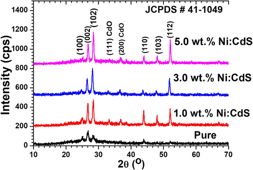
XRD patterns of pure and Ni doped CdS thin films with different Ni doping concentrations.
Films structural parameters for all composition are listed in Table 1 where they reveal the variation with Ni doping content in CdS.
Samples (Ni:CdS)
a = b (Å)
c (Å)
c/a
V (Å)3
Dave (nm)
δave (nm−2) × 10−3
εave × 10-2
N × 104
0.0 wt% Ni:CdS
4.11170
6.67526
1.62348
97.73328
13.93
5.23
1.09
1.45
1.0 wt% Ni:CdS
4.11304
6.67364
1.62256
97.77323
19.46
2.65
0.77
3.94
3.0 wt% Ni:CdS
4.09824
6.80232
1.65982
98.94241
21.28
2.28
0.72
5.10
5.0 wt% Ni:CdS
4.15204
6.72848
1.62053
100.45467
23.05
1.96
0.67
6.38
3.2 Vibrational study
Further confirmation of phase and purity of CdS material, as grown films of Ni:CdS compositions with 1.0, 3.0 and 5.0 wt% were investigated using Raman spectroscopy. Fig. 2 illustrates the Raman spectroscopy of the films with different Ni doping concentrations. As shown in Raman spectra, a clear peak can be seen at 301.61 cm−1 and 602.34 cm−1 from Fig. 2 (Zelaya-Angel et al., 1997, Farid et al., 2012). The vibrational mode at 301.61 cm−1 corresponds to the 1LO longitudinal optical phonon vibrational mode and the second mode at 602.34 cm−1 corresponds to the first harmonic (2LO) mode, which belongs to the characteristic vibrational mode of hexagonal wurtzite structure CdS. A significant effect of Ni doping on Raman peak was observed, as increasing the concentrations of Ni doping FWHM of ILO peak gives rise to the increase in intensity of the peak. This suggests the noticeable variation of structural change with Ni incorporation in CdS. Similar changes in structural quality of films were confirmed through XRD analysis.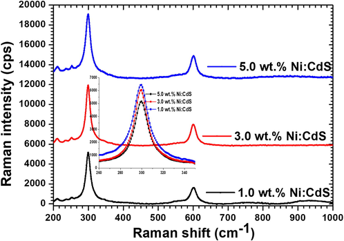
Raman spectra of Ni doped CdS thin films with different Ni doping concentrations.
3.3 Compositional and homogeneity studies
The energy dispersive X-ray spectra (EDX) of a 5.0 wt% doped film with mapping are shown in Fig. 3. A clear information about the doping of Ni can be seen from Fig. 3. All elements were detected in EDX spectra which are part of films composition. No traces of impurities were recorded in EDX spectra which confirms the growth of pure compounds in the films. Surface morphological properties of films were investigated using FESEM. Fig. 4 shows the FESEM images of Ni doped CdS thin films with different concentrations. The distribution of the particles on the surface is compact and clear shape like concrete which confirms the hexagonal phase of the particles. The particle size of films highly varied with the Ni doping as can be seen in Fig. 4. The particle size of film increases with the increase of Ni doping concentration which shows well agreement with XRD results.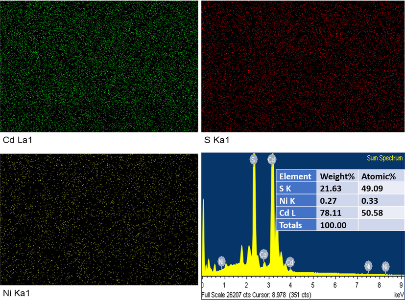
EDX mapping and spectra of 1 wt% Ni doped CdS thin films samples.
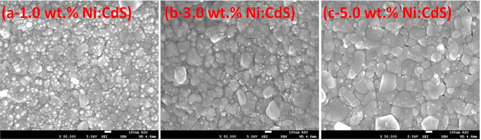
FESEM images of Ni doped CdS thin films with different Ni doping concentrations.
3.4 Optical study
3.4.1 Absorption-transmittance and reflectance analyses
The electronic structure modification with Ni doping of films were studied using UV–vis-Nir spectroscopy. Fig. 5 shows the absorbance (A), transmittance (T), and reflectance (R) spectra of pure and Ni doped CdS films in the range of 190–2500 nm (a–c). All films showed strong absorbance in visible region as revealed in the Fig. 5(a). The band edge of film changes significantly as a result of the replacement of Cd atoms with Ni in CdS system. The band edge of the doped films becomes sharper as Ni incorporated in the CdS lattice in comparison with the pure films. This implies the improvement in electronic structure with Ni doping. In addition, the doped films showed that there is an enhancement in the absorbance in 600–900 nm regions with the increase in Ni doping concentrations. Pure and Ni doped films transmittance spectra are shown in Fig. 5(b). Films have 40–50% transmittances in the visible region and reduced with the incorporation of Ni in the CdS system as shown in Fig. 5(b). The reflectance percentage of the films are illusterated in Fig. 5(c). The impact of Ni doping on reflectance in the region 400–600 nm is minimal, however, after 600 nm the reflectance of the films enhanced.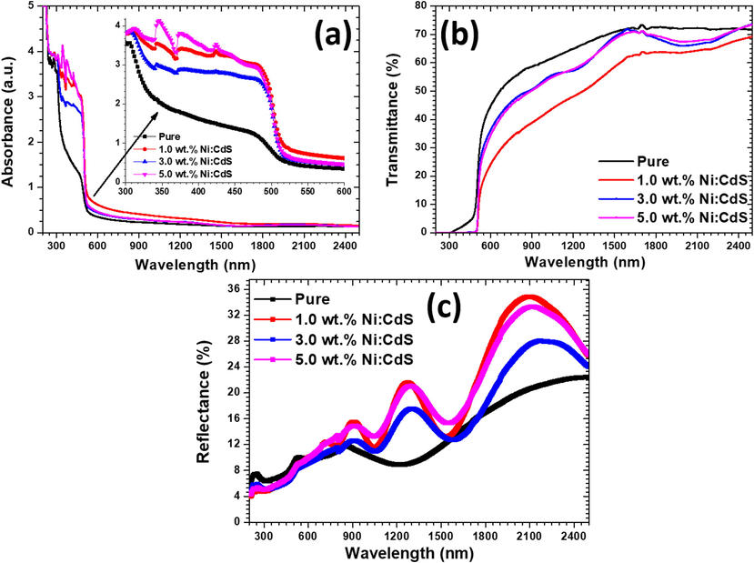
(a) Absorbance (b) Transmittance (c) reflectance of pure and Ni doped CdS thin films.
3.4.2 Energy gap-absorption index-refractive index-dielectric analyses
The optical band gap of all films was calculated and analysed in correlation of Ni doping concentrations. The well-known Tauc’s formula
was used to calculate the band gap energy of the pure and Ni doped CdS thin films (Lokhande and Pawar, 1983; Wei et al., 2017). Fig. 6 demonstrates the plots of (αhν)2 versus hν for the pure and Ni doped CdS films with different concentrations. Fig. 6 also exhibits the typical optical band gap energies of the fabricated thin films. As a result, the optical band gaps were obtained by extrapolating the linear portion of the plots to zero absorption coefficient on the x-axis. The calculated optical band gap of the deposited pure CdS thin film was 2.39 eV while the calculated band gaps for the 1.0 wt%, 3.0 wt%, and 5.0 wt% Ni-doped CdS thin films were 2.42, 2.43, and 2.42 eV, respectively (Chand and Ghosh, 2018; Rmili et al., 2013). A significant impact of Ni doping on the value of the band gap can be seen clearly from Fig. 6. Therefore, a blue shift was observed in the band gap when Ni doping in CdS system. Fig. S1(a) (see supporting data file) shows the refractive index (n) and absorption coefficients (k) of the pure and Ni doped films with different doping concentrations. The Fresnel equation
was used to calculate the refractive indice of all films in 190–2500 nm range (El-Bana et al., 2017; Viezbicke et al., 2015). By increasing Ni doping concentrations, all films showed a substantial rise in refractive index in the near infrared range. For all the compositions, n values were computed in the range of 1.39–3.88. In addition, the absorption indice (k) of all films were calculated using the formula:
, where α denotes the absorption coefficients and wavelength of spectrum is referred as λ (AlFaify et al., 2020). The absorption indices of the films was calculated using the absorption coefficients ranging from 0.07 to 0.32. Fig. S1(b) (see supporting data file) depicts the real (ε1) and imaginary (ε2) parts of the complex dielectric constants of the pure CdS and different concentration of Ni doped CdS thin films. The relation of complex dielectric constant is given as ε*=ε1 + iε2. The calculations of the real and imaginary parts of dielectric constant were obtained via equations ε1 = n2-k2 and ε2 = 2nk (Lam et al., 2017, Halge et al., 2020).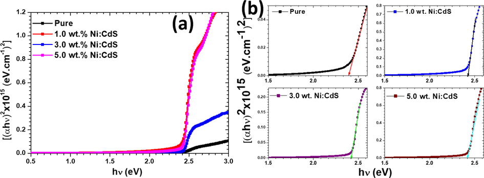
(αhν)2 vs. hν plots for pure and Ni doped CdS thin films with different Ni doping concentrations.
3.5 Nonlinear properties
CdS is a promising nonlinear optical material and has potential applications in optical limiting and laser-controlled devices. In the present work, the impact of Ni doping on nonlinear optical properties were also investigated as a function of Ni doping concentrations. The ccurrence of nonlinear polarization on the material exposed to the intense light is the main cause of 3rd-order nonlinearity development. The polarization of materials usually can be expressed via the relation P = εoχE, where, εo stands for the free space permeability and E stands for the electric field intensity and optical susceptibility (Raj et al., 2020). Χ is expressed by the relation , where , is the linear part of optical susceptibility and , is the nonlinear part i.e., the are the second and third order optical susceptibilities. The general relation of the refractive index n(λ) is given by the equation , where the components of n(λ) have obeyed some mathematical conditions: n0(λ)»n2(λ), i.e., n(λ) = n0(λ) and (E2) is the mean square of an electric field. The well-known relation derived from the refractive index was used to calculate the linear optical susceptibility χ(1) for the medium (Gunasekaran et al., 2020). The third order nonlinear susceptibility was obtained through the relation: . The nonlinear refractive indices of the films were estimated using the formula: (Thangaraju et al., 2020).
The χ(1), χ(3) and n2 versus photon energy graphs of the pure and Ni doped CdS thin films are shown in Fig. S2(a-c) (see supporting data file). The values of the linear optical susceptibility were found in the range of (1.09–0.07 esu). In the energy range 0.5–2.5 eV, the linear optical susceptibility increases with increasing Ni doping concentration and decreases in the 2.5–6.0 eV region. As can be seen in Fig. S2(b) (see supporting data file), the optical third order nonlinear susceptibility showed a sharp peak in 0.5–1.0 eV energy region, which suggests that the Ni:CdS material, is selective for nonlinear optical applications in this energy range. The third order nonlinear optical susceptibility values were obtained in the range of 2.12 × 10⁻¹²–2.65 × 10⁻¹⁰ esu over the energy range 0.5–6.0 eV. Similar values of χ(3) were previously reported by various research groups in CdS thin films (Abhiram et al., 2021; Marnadu et al., 2021a,b; Sasikala et al., 2021; Marnadu et al., 2020). The sharp peak was observed at 0.75 eV for the sample doped with 1 and 5 wt% and vales of n2 were about 2.01 × 10⁻¹¹–2.61 × 10⁻⁹ in 0.50–6.0 eV energy range. The investigation of the nonlinear optical parameters confirms that the Ni doped CdS films are the best material for nonlinear optical applications.
3.6 Photoluminescence
Further insight studies of Ni doping on the electronic structure of the CdS thin films, showed the recording of the photoluminescence at room temperature (RTPL). The pure and Ni doped CdS RTPL spectra of all films are shown in Fig. 7. Characteristics near band edge peak (NBE) of CdS can be observed in the range of 537–540 nm from Fig. 7 (Amiri and Alizadeh, 2020). This peak is corresponding to the inter band transition. On the other hand, low intense broad peak was observed in the 670 nm region, which might be attributed to the cadmium interstitial Cdi and SV vacancies that are created during the development of the films (Lou et al., 2016). A significant effect of Ni doping is shown on the emission spectra of the films. A clear blue shift can be seen in the NBE peak along with the enhancement in th peak intensity centred at 670 nm.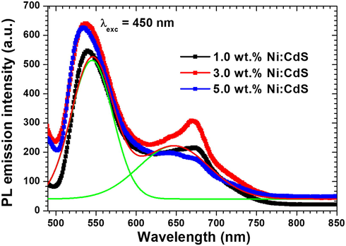
Room temperature photoluminescence of pure and Ni doped CdS thin films.
3.7 I-V electrical studies
Fig. 8(A) shows a schematic depiction of the white light photodetector based on the Ni:CdS thin films. The current–voltage (I-V) properties of the pure CdS and Ni:CdS thin films with various Ni doping concentrations are shown in Fig. 8B(a–d). To analyse photo response of the device, the photocurrent of each Ni:CdS thin film-based photodetector was measured using various light intensities (like 0, 210, 310, 550, 920, 1450 lx). By increasing the applied voltage from 0 to 5 V, the obtained photocurrent was found to increase linearly with the applied potential. Moreover, each photocurrent values were enhanced while increasing the intensity of the light (white light). When the light is switch ON, the photo-excited holes (h+) transfer to the surface and release the absorbed oxygen (O) ions by the recombination of the charge carriers. Therefore, an unpaired electrons effectivly improved the conductivity of the Ni:CdS films (Lam et al., 2017; Halge et al., 2020). The higher intensity of 1450 lx exhibited a maximum photocurrent when compared to dark condition, which indicates the superior photoconducting nature of the Ni:CdS thin film-based photodetector. Owing to the separation of photo rerated electron–hole (e−–h+) pairs, the resultant Ni:CdS based photodetector exposed an outstanding photoresponse (Halge et al., 2020; Marnadu et al., 2019). It is evident from Fig. 8B(a–d), that the incorporation of Ni ions on the CdS matrix effectively improved the photocurrent of the Ni:CdS films from 10−8 to 10−6 A. Interestingly, the Ni:CdS film was achieved higher photocurrent of 3.5 × 10⁻⁶ A at 5 V. These results strongly suggested that the current Ni:CdS film-based photodetectors are superiorly sensitive with Ni doping level, light intensity and applied voltage. The higher generation of photocarriers under light environment, less recombination of charge cupules, more separation electron-hole pairs and their lifetimes are the responsible for attaining the higher photocurrent (Gunasekaran et al., 2020; Thangaraju et al., 2020; Abhiram et al., 2021). Fig. 9(a) demonstrates the variations of the photocurrent (ln IPh) with the external light intensity (ln F). This result obviously shows that the photocurrent of the pure CdS and Ni:CdS films were increased steadily with the external light intensity due to the higher creation of the photocarriers under the white light. Also, we noticed that there is a large difference in the photocurrent after incorporating Ni ions into the host CdS system. The addition of foreign Ni ions improved the crystallites size of the CdS films, which were confirmed by the XRD results (Marnadu et al., 2021a,b; Sasikala et al., 2021). If the crystallite size of the coated thin film is increased, the grain boundary of each film will be reduced. Moreover, our SEM images also confirmed that the grins are strongly interconnected together without any gap. As a result, the electrical conductivity of the films was increased (Marnadu et al., 2021a,b; Sasikala et al., 2021; Marnadu et al., 2020). Therefore, the Ni:CdS films exhibited superior photocurrent after Ni doing (Fig. 9a). It is worth to mention here, that the dark surface resistivity was gradually reduced while increasing the Ni concentration which is shown in Fig. 9(b). The 3% of NI:CdS films recorded to a minimum surface resistivity of 1.54 × 10⁷ Ohm/cm. Thus, this lower the surface/volume resistivity of the Ni:CdS films indicating the higher conductive of the material. Besides, the photo surface resistivity of each films decreased continuously with Ni concentration and light intensity as displayed in Fig. 9(c). The higher intensity of 1450 lx showed a lower photo surface resistivity relatively with other intensity. A less photo surface resistivity of 1.36 × 10⁶ Ohm/cm was observed for higher Ni concentration of 3%. We observed that the 3% Ni:CdS films reduced the surface resistivity to about 1.41 × 10⁷ Ohm/cm after light illuminating condition. This result approves the good photoresponce of the formed Ni:CdS thin films. The photosensitivity of the Ni:CdS films was strongly varied with the Ni concentration and the intensity of light as displayed in Fig. 9(d). The average value of the photosensitivity seems to be improved when the light intensity increases. This result was mostly ascribed due to the efficiency and improved mobility of the created charge carriers in the photoconductive Ni:CdS film (Amiri and Alizadeh, 2020). The pure CdS films have the highest photosensitivity of 32.995, which is related to the reduction of surface sulphur vacancy defects, which improves the concentration of the photogenerated free carriers (Lou et al., 2016). This is clearly known that the more creation of photocarriers after illuminating sufficient light energy is accountable for this improvement. The diode's photosensitivity is mostly related to the intensity of incident light, reduced charger cupule recombination, and the Ni:CdS film's absorption rate. From the I-V results, we proved that each Ni:CdS films are highly sensitive for both light and Ni concentration.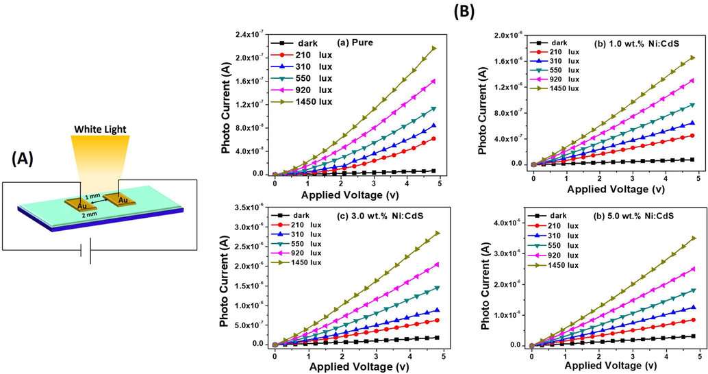
(A) Schematic diagram of the fabricated device and (B) I-V charactrusrucs of the Ni:CdS films based photodetector.
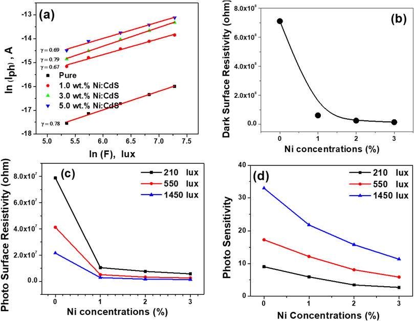
(a) Recombination plot, (b) dark surface resistivity vs. Ni concentrations, (c) photo responsivity vs. Ni concentrations and photosensitivity vs. Ni concentrations for Au/CdS/Au and Au/Ni:CdS/Au photodetector.
4 Conclusion
A successful development of pure CdS and different concentrations of Ni doped CdS films through a facile and low-cost spray pyrolysis technique. Furthermore, the Au/CdS/Au and Au/Ni:CdS/Au photodetectors devices were also developed. Phase/elemental composition/dopant homogeneity in the final films was investigated. Nanograins like particles are formed in the grown films observed by the SEM analysis. The detailed optical parameters such as energy gap, absorption index, refractive index, dielectric constant etc. were determined and discussed. The PL emission shows an intense band at ∼540 ± 6 nm at 450 nm excitation wavelength. The detailed I-V electrical performance under dark & photo was studied and the recombination behaviour, surface resistivity and photosensitivity of Au/CdS/Au and Au/Ni:CdS/Au photodetectors were investigated. The device surface resistivity in dark is noticed to be higher than photo one. The device showed an enhancement in the photosensitivity from 10% to 35% when the light intensity was increased to 1450 lx. The results indicate that the developed photodetectors might be a good contender for using in optoelectronic.
Acknowledgements
Authors would like to acknowledge the support of the Ministry of Education, Kingdom of Saudi Arabia for this research through a grant (PCSED-012-18) under the Promising Centre for Sensors and Electronic Devices (PCSED) at Najran University, Kingdom of Saudi Arabia. Authors are highly thankful to Dr. Aslam Khan, King Saud University for his kind help in performing the FESEM/EDX analysis.
Data availability statement
The raw/processed data required to reproduce these findings cannot be shared at this time as the data also forms part of an ongoing study.
Declaration of Competing Interest
The authors declare that they have no known competing financial interests or personal relationships that could have appeared to influence the work reported in this paper.
References
- J. Nanopart. Res.. 2021;23:83.
- J. Mater. Res. Technol.. 2019;8:2021-2030.
- Opt. Laser Technol.. 2020;126:106122
- Mater. Sci. Semicond. Process.. 2020;111:104964
- Phys. B. 2019;555:145-151.
- Surf. Interfaces. 2021;23:100992
- Optik. 2018;161:44-53.
- Mater. Chem. Phys.. 2000;63:163-166.
- J. Mater. Chem. A. 2020;8:20658-20665.
- J. Appl. Phys.. 2007;101:013712
- J. Alloy. Compd.. 2017;705:333-339.
- J. Appl. Phys.. 2012;112:043907
- AIP Conference Proceedings. American Institute of Physics; 2012. p. :45-48.
- Surf. Interfaces. 2020;20:100622
- ACS Appl. Electr. Mater.. 2020;2:2151-2154.
- Energy Procedia. 2013;33:203-213.
- J. Ovon. Res.. 2014;10:185-190.
- Int. J. Mol. Sci.. 2011;12:6320-6328.
- Appl. Surf. Sci.. 2019;476:374-377.
- Sens. Actuators, A. 2021;319:112531
- Thin Solid Films. 2008;516:7306-7312.
- Mater. Sci. Eng., B. 2010;174:145-149.
- J. Electron. Mater. 2019:1-11.
- Mater. Res. Express. 2018;5:036406
- Semicond. Sci. Technol.. 2021;36:065022
- Opt. Mater.. 2021;116:111086
- Nanoscale Res. Lett.. 2017;12:1-7.
- Mater. Res. Bull.. 1983;18:1295-1301.
- Nanoscale. 2016;8:5219-5225.
- J. Alloy. Compd.. 2017;691:399-406.
- Appl. Surf. Sci.. 2019;480:308-322.
- J. Inorg. Organomet. Polym Mater.. 2020;30:731-748.
- J. Inorg. Organomet. Polym Mater.. 2021;31:2280-2292.
- J. Inorg. Organomet. Polym Mater.. 2021;31:2280-2292.
- J. Mater. Sci.: Mater. Electron.. 2017;28:7749-7759.
- Mater. Sci. Semicond. Process.. 2018;79:74-91.
- J. Mater. Sci.: Mater. Electron.. 2018;29:20439-20454.
- J. Alloy. Compd.. 2019;779:762-775.
- J. Alloy. Compd.. 2021;888:161568
- Curr. Appl. Phys.. 2019;19:1136-1144.
- RSC Adv.. 2014;4:44547-44554.
- Opt. Mater.. 2019;92:319-329.
- J. Appl. Spectrosc.. 2020;87:35-40.
- New J. Chem.. 2020;44:7708-7718.
- J. Alloy. Compd.. 2013;557:53-59.
- Mater. Res. Express. 2019;6:056414
- Inorg. Chem. Commun.. 2021;130:108701
- Chin. J. Phys.. 2020;63:51-62.
- RSC Adv.. 2017;7:53951-53962.
- CrystEngComm. 2020;22:525-533.
- Mater. Res. Express. 2019;6:1050c1058.
- J. Superlattices Microstruct.. 2015;85:237-247.
- Physica Status Solidi B. 2015;252:1700-1710.
- Physica Status Solidi A. 2006;203:2018-2023.
- Sens. Lett.. 2019;17:804-806.
- Phys. B. 2017;525:98-103.
- Microelectron. Eng.. 2016;157:64-70.
- J. Alloy. Compd.. 2019;776:1056-1062.
- Solid State Commun.. 1997;104:161-166.
Appendix A
Supplementary data
Supplementary data to this article can be found online at https://doi.org/10.1016/j.jksus.2021.101638.
Appendix A
Supplementary data
The following are the Supplementary data to this article: