

Translate this page into:
Highlighting some layers properties in performances optimization of CIGSe based solar cells: Case of Cu(In, Ga)Se–ZnS
⁎Corresponding author. nyafridolin@yahoo.fr (Tchangnwa Nya Fridolin)
-
Received: ,
Accepted: ,
This article was originally published by Elsevier and was migrated to Scientific Scholar after the change of Publisher.
Peer review under responsibility of King Saud University.
Abstract
In this research work which is based on recent studies, we investigated the effects of the physical properties of the Zinc Sulfide (ZnS) buffer layer such as electronic affinity, doping concentration and thickness on the electrical parameters of a defined solar cell structure. These properties values, combined with those of the CIGSe absorber layer and other materials that make up our cell, provide vital information on the optimization of the layer properties that enhance the efficiency of the CIGSe based ultra-thin solar cells. After a judicious choice of the input parameters of the materials constituting our solar cell device, we obtained employing SCAPS numerical simulation software, electrical parameters more interesting than those found in the literature. In particular, for 5 nm thickness of the ZnS buffer layer and 500 nm thickness of the CuIn0.7Ga0.3Se2 absorber layer, we obtained an efficiency η = 21.42% and a fill factor FF = 82.16%. For 5 nm thickness of the ZnS buffer layer and 2500 nm thickness of the CuIn0.7Ga0.3Se2 absorber layer, we obtain an efficiency η = 26.30% and a fill factor FF = 85.15% with a good choice of others material properties such as intrinsic doping concentration, electrons and holes mobility. A good knowledge of the exact parameters of simulations, allowed us to determine the values of the optimal properties of the Cu(In, Ga)Se–ZnS solar cell, useful for their physical implementation.
Keywords
ZnS
CIGSe
Solar cell
SCAPS numerical simulation
Recombination
Efficiency
Fill factor

1 Introduction
This last decade has been marked by a dizzying rise in the field of photovoltaics and precisely in the CIGSe based thin-film solar cells. A record of 22.6% efficiency was achieved by the ZSW (Zentrumfür Sonnenenergie & Wasserstoff Forschung – Germany) center at the end of 2016 and the research was oriented towards thickness reductions; window and buffer layers substitution; optimization of efficiency and stability of photovoltaic devices. Among the alternative materials recognized by the scientific community, zinc sulphide ZnS is illustrated as the most promising one, although the highest yield obtained with it to date does not exceed 22% (Martin Green et al., 2016). In the process of reducing the thickness of the layers, numerous works have been identified. Notably the work of Mostefaoui et al. (2015), who arrived at a yield of 20.75% with only 1 μm of absorber layer thickness and using ZnS as buffer layer. Our recent work allowed us to obtain a very promising yield of 22.62%, with nanoscale thicknesses for the different layers and using CdS as buffer layer. In the following, we highlight using SCAPS numerical simulation software, the influence of the values of certain properties of layers (ZnS and CIGSe) and interfaces mainly, their electronic affinity, thickness and intrinsic doping level on the performances of our solar device. Our main objective in this study is to determine the values of the properties of the material which allow us to obtain good and stable solar devices with better performances and also to define the critical values of the properties beyond which we can indeed obtain a good efficiency but unstable and bad device (Powalla et al., 2006; Nakada and Kunioka, 1999; Liao and Rockett, 2003; Schmid et al., 1993; Okano et al., 1998; Romero et al., 2003; Jiang et al., 2003; Li et al., 2012; Minemoto et al., 2001; Pogrebjak, 2011, 2012) (Fig. 1).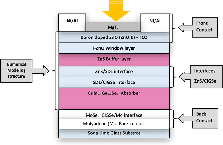
One-dimensional structure of the cell.
2 Material and methods
2.1 CIGSe – ZnS cell structure
The structure of the cell that we model for our simulations is the following:
2.2 The ZnS/SDL and SDL/Cu(In, Ga) Se2 interfaces
In the work of Soumaila et al., and in recent work (Soumaila et al., 2014; Tchangnwa and Nya, 2017), the beneficial effect related to the existence of the Surface Defects Layer (SDL) on the performance of the cell is known. Indeed, SDL is due to the presence of an N-type (N-SDL) Indium-enrich layer on the surface of the P-type absorber layer and this layer is responsible for the cleavage observed at the band gap level and it would have the effect of improving the properties of the cell at the junction. Touafek and Mahamdi (2014) interprets the SDL as a Copper-poor layer on the surface of the absorber layer. The two interpretations are complementary, the N-SDL therefore has a structure similar to the absorber layer, but it has different properties. Consequently, the P-N heterojunction in the CIGSe cell is indeed a homo-junction which is formed between (P-CIGSe) and (N-SDL) and it is completely localized in the CIGSe structure. Thus, at the ZnS/CIGSe junction, we may have two important interfaces: ZnS/SDL and SDL/CIGSe and all the electrical properties of the SDL layer are identical to those of the absorber layer, except for parameters such as band gap, doping concentration and the mobility of charge carriers.
2.3 Factors of loss of performances
By reducing the thicknesses to nanoscale, the current generation mechanisms face reverse processes tending to reduce the performance and quality of the photovoltaic cell device. These are recombinations and defects states.
2.3.1 Recombinations
These mechanisms are characterized by their rates R which represents the number of recombinations per unit time and per unit volume of the semiconductor material and by the lifetime of the charge carriers. There are three main recombination mechanisms in literature: Auger recombination , radiative recombination , Shockley-Read-hall recombination . As part of our work, only the first two will be studied. It is important to remember their mathematical expressions.
After all the necessary approximations made we have:
2.3.2 Highlightsing of the effects of defects states in the cell
The characteristics of semiconductor materials are strongly influenced by impurities or defects. The latter are most often added in order to increase the electrical conductivity or to control the lifetime of the material. Certain defects appear during the different processes of preparation and deposition of the materials. They act as factors of loss within the device (Benosman et al., 2003).
2.3.2.1 Highlighting of the defects states at the ZnS/SDL interface
The main function of the ZnS buffer layer in the structure is to form the heterojunction with the CIGSe absorber layer and protect the SDL. Therefore, the deposition method must be chosen so that it minimizes the density of the defects at the interface. In the ideal case, which imply that, without the effects of defects at the interface, the positive charges formed by the ZnO: B/i-ZnO/ZnS layers on the other side of the junction compensate the negative charges in the space charge region (SCR) of width
which is almost wholly localized in the absorber layer. At equilibrium we have:
From this equation, it can be seen that the introduction of a negative charge materialized defect state for example at the interface, reduces the width of the SCR in the absorber layer. As a consequence, it will lead to increasing the rate of recombination at the ZnS/CIGSe interface and thus reducing the cell device performance. Touafek and Mahamdi (2014), who worked with the CdS/CIGSe, confirmed this assertion.
2.3.2.2 Highlighting defects states at the SDL/CIGSe interface
In fact, the presence of defects in themselves is inevitable and is not as damaging as is thought. It is when their density increases that their harmful effects are felt. An excess of localized defects states at the SDL/CIGSe interface constitutes centers of recombination at this interface and therefore points of manifestation of the mechanisms of losses in performances. Touafek and Mahamdi (2014) studied the effect of excess density of defect states at the SDL/CIGSe interface for a cell using the CdS as buffer layer. They showed that for a defect density of 1012 cm2 and an electron-hole capture section through the interface of 10−12 cm−2, the efficiency dropped from 18.9% to 14%. Wan Fucheng et al. (2014) in their work show through the AMPS-1D numerical simulation program that the effects of defects states almost always act as loss factors on solar cell performance. The following conclusion was drawn: When the defect state densities are less than 1014 cm−3 in the absorber layer and less than 1018 cm−3 in the buffer layer, the defect states have very little influence on the performance of the device.
2.4 Choosing certain ZnS properties
2.4.1 Reasons for choosing ZnS
ZnS has intrinsic properties which make it a material of choice in the search for good performance in the CIGSe-based thin film chain. It is recognized as having the following properties: It is non-toxic to the environment; It has a wide band gap, which allows the transmission of photons of higher energy, thus increasing the absorption of the light spectrum in the absorber layer; It has a relatively high exciton binding energy (34 meV); its shear modulus (which indicates the stability of the crystal) is very large, close to 45.5 Gpa; its refractive index is high (2.35); its structure exhibits a better lattice matching with absorbers having energy bands in the range (1,2–1,5 eV) (BENGHABRIT, 2015); its constituents are abundant in nature (Zinc and sulfur) and finally it has a high mobility of electrons (165 cm−2/Vs).
2.4.2 Choosing of certain properties
In the literature, there are two ZnS crystallographic structures, the Zinc Blende structure or cubic structure and the hexagonal structure. Won Song et al. (2012) in their work, show that the cubic structure, more stable at ambient temperature, forms a better lattice matching with the chalcopyrite structure of CIGSe. It is the properties of this structure that will be taken into account. It allows us to record as the band gap energy value and as the value of the dielectric constant .
2.5 Numerical tools and input parameters of materials
We have modeled our solar cell device by using the version 3.3 of the one-dimensional numerical simulation software SCAPS (Burgelman et al., 2000) and the input parameters are recorded in Table 1.
Material properties
CIGSe
SDL
ZnS
i-ZnO
ZnO:B
Layer thickness (nm)
variable
10
variable
50
200
Band gap
(eV)
1.2
1.45
3.68
3.4
3.3
Affinity
(eV)
4.5
4.5
4.3
4.55
4.55
Dielectric relative constant
13.6
13.6
8.3
10
10
Conduction band effective density of states: Nc
2.1018
2.1018
2.2 1018
3.1018
3.1018
Valence band effective density of states:
1.1017
1 1017
1.5 1019
1.8 1019
1.8 1019
Electron thermal velocity
107
107
107
107
107
Hole thermal velocity
107
107
107
107
107
Electron mobility
50
100
165
100
100
Hole mobility
20
1.25
5
31
31
BULK DEFECT PROPERTIES
Type
ACCEPTOR (A)
DONNOR (N)
DONNOR (N)
DONNOR (N)
DONNOR
(N)
Density of defect
–
–
–
–
–
Doping concentration
1015
5 1015
1017
1017
1020
INTERFACE PROPERTIES
Interface state
CIGSe/SDL
SDL/ZnS
Interface Conduction bandoffset:
(eV)
0.3
0.3
Defects density and type
I N(cm2)
1010 (Neutral)
2.1012 (Neutral)
Capture cross-section electrons:
10−19
10−15
Capture cross-section hole:
10−19
10−15
3 Results and discussions
3.1 Optimization of ZnS properties
3.1.1 Optimal value of ZnS electronic affinity
We determine the optimum value of the electronic affinity of ZnS in order to obtain better results. To do this, we consider as the minimum value of
, that obtained following the work of Al-Ani et al. (2006) that is to say 3.9 eV and as maximum value, that obtained following the work of Ramli et al. (2013) that is to say 4.5 eV. We study the influence of the value of
on the output parameters of the cell (efficiency and fill factor) by varying it in the range of values previously found for
which allows us to plot the following Fig. 2a and b.
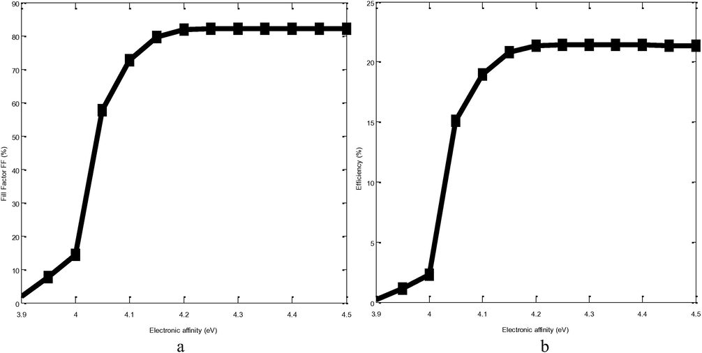
The figures Fig. 2a and b above show that the optimum value of the ZnS electronic affinty for recording the best performance of our solar cell is defined for . This result is in very good agreement with the previous results reported in literature (Al-Ani et al., 2006). The maximum of the parameters is obtained for . This is the optimum value of the electrical susceptibility of ZnS according to our solar cell device.
3.2 Influence of the doping concentration of the absorber layer on the parameters of the cell
Our recent work with the CdS as buffer layer (Tchangnwa and Nya, 2017) has shown that, beyond a concentration of holes = 0.8 1014 cm−3, the overall parameters of the cell degrade considerably. Soumaila et al. (2014) have shown in their work that beyond , the voltage reaches saturation independently of the thickness of the absorber layer. These works mentioned above allow us to study the influence of the intrinsic doping level of the absorber layer on the output parameters of the cell by varying first of all between and , and then between and , the thicknesses of the absorber layer between 100 nm and 2500 nm and the thicknesses of the buffer layer between 1 nm and 50 nm. This is done in order to show more precisely the influence of the absorber intrinsic doping level on the properties of the materials.
It appears from these figures that the photovoltaic parameters of the cell are globally influenced by the intrinsic concentration of the acceptors. The open-circuit voltage (Fig. 3a) increases substantially with the increase of the doping level
for a fixed value of the thickness of the absorber. By simultaneously increasing the thickness of the absorber, it is realized that for the same value of
, the values of
increases, the same is true for the efficiency (Fig. 3d). Conversely, the circuit current
(Fig. 3b) and the fill factor (FF) (Fig. 3c) decrease significantly with the increase of
.
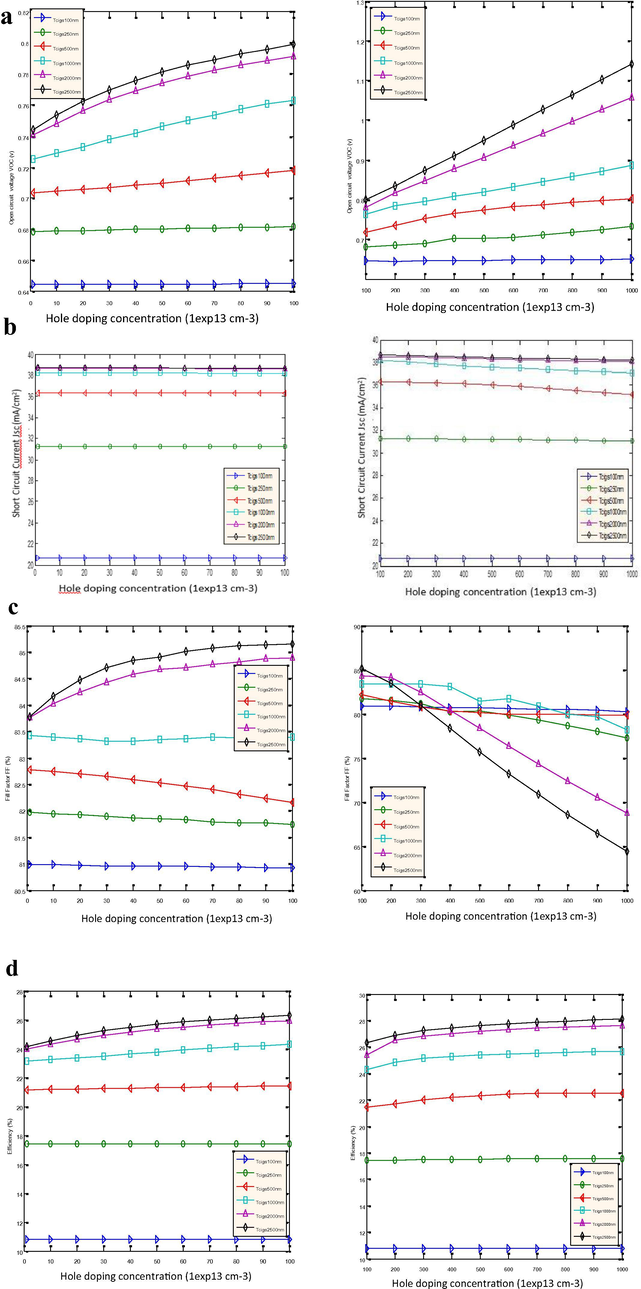
By setting the value of , and by varying , the output parameters of the cell are almost constant. This implies that, the doping level of the absorber has no influence on the output parameters of the cell when only varies.
When , the doping level almost does not influence the output parameters of our cell. The conversion efficiencies (Fig. 3d) and the fill factor (Fig. 3c) remain almost constant. However, for the fill factor (Fig. 3c) begins to decrease with increase of .
When , a significant increase in the output parameters of the cell can be seen from the value .
For
, and for
, the parameters of the cell are globally interesting because
(Fig. 3a), where
is the saturation voltage of our device. In addition, the short-circuit current is at its maximum value
(Fig. 4b) and the values of the fill factor (Fig. 3c)
. This observation is important because it will allow to circumscribe the optimal value of
.
For , the overall performance of the cell increases significantly. One would be tempted to believe that the best performances can be obtained with a high level of intrinsic doping recorded in the absorber layer, however two factors limit the adoption of a high level of doping: The quality factor Fig. 3c decrease significantly characterizes the poor quality and instability of the solar device in question; For and considering , saturation is automatically reached. Thus for we have , .
Indeed, according to the mathematical expression given by formula (2), we note that the lifetime of the electrons will decrease when the doping concentration P of CIGSe increases, so according to the mathematical expression (4) the lifetime of electrons is inversely proportional to the square of the hole density and therefore of the doping concentration. It is therefore necessary, when controlling the intrinsic doping level of the absorber, to control the concentration of the acceptors at an optimal minimum level, the benefits of higher doping are limited by the Auger and radiative mechanisms.
Moreover, for , the performances of the cell are globally very interesting. This would probably justify why Daouda et al. (2015) obtained a good yield (18.6%) by working with . However, they quickly reached saturation as soon as . One of the aims of this work is to propose a solar cell structure which can be manufactured with a thickness while maintaining good performances. The analysis of the different graphs shows that the optimal intrinsic doping level of CIGSe is .
It has also been shown that the majority of recombination occurs in the CIGSe volume, ie they are dominant in the SCR, and in this region, the open circuit voltage is expressed as:
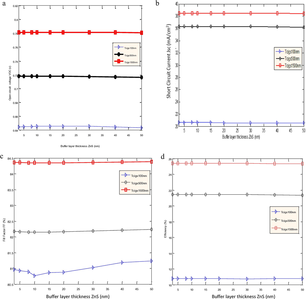
3.3 Influence of the thickness of the buffer layer on the parameters of the cell
Cho et al. (2016) concluded at the end of their work that a thickness of 8 nm ZnS buffer layer allowed them to obtain good yields, ie 12.6% (April 2016). They obtained this result by optimizing the ZnO/ITO window layer deposition process. However, its device thus set up, although moderately satisfactory on the yield side, did not make it possible to obtain a stable and better structure due to the low value of the fill factor FF = 66.8%. Moreover, its results did not take into account the joint effects of other materials properties such as intrinsic doping, thickness values of the absorber and the existence of the SDL. In this section, the influence of the ZnS thickness on the output parameters of the cell is determined by fixing and by varying = 100 nm, 500 nm and 1500 nm.
Two major facts are highlighted in this section: The conversion efficiency (Fig. 4d), the short-circuit current (Fig. 4b) and the open-circuit voltage (Fig. 4a) all decrease with the increase of ; The fill factor (Fig. 4c) decreases for , then it grows from the value .
Increasing does not increase the electrical output parameters of the cell, but it allows to have a good fill factor that shows a more stable structure but less good performance. The optimal value interval of . Indeed, the smaller the the more the majority carriers that are the photo-generated electrons are collected. Literature proposes as a standard buffer layer thickness for CIGSe thin films, 40 nm < < 60 nm, probably to justify the design of more stable structures. In the challenge of reducing the thickness, while maintaining good output parameters, it is important to find a better compromise between Thickness-Yield-Quality-Feasibility of the structure. The best performances of our cells are recorded for = 5 nm. This result is not very far from those of Cho et al. (2016).
3.4 Influence of the thickness of the absorber layer
The aim here is to evaluate the effect of the thickness of the active layer on the conversion parameters of the cell with the optimized properties of the other layers. The standard thickness of a Cu (In, Ga) Se2 absorber in CIGSe solar cells varies between 2000 nm and 3000 nm. By taking as input parameters the optimal values of the properties of the other layers already chosen, this section defines the thickness interval in which the best performances are obtained. To this end, we study the effects of increasing the thickness of the absorber layer on the output parameters of the cell.
There are two main areas of interpretation, the first for 100 nm ≤ ≤ 500 nm and the second for 500 nm < < 2500 nm. It is important to note first that, the parameters (Jsc, Voc, FF, η) increase significantly with the increase of .
For
[100; 500 nm] the short-circuit current Jsc, is the most affected parameter, its value goes from 20.65 mA/cm2 for
to 36.31 mA/cm2 for
= 500 nm. Which gives a gain of 16 mA/cm2 (Fig. 5b). This increase is due to the fact that the width of the SCR is increasingly completely embedded in the larger volume of the absorber layer, thereby reducing the rate of backward recombinations at the CIGSe/Mo interface. Similarly, between [100; 1000 nm], the
increased from 0.65 to 0.76 V. That is to say an increase of 0.13 V!! (Fig. 5a), which make it possible to pass the efficiency from 10.78% to 24.31% or a gain of almost 14% (Fig. 5d) and finally to obtain an impressive fill factor of 83.4% (Fig. 5c. But why do we record such good values of all the output parameters of our solar cell device? It is important to remember that we work with optimized values of materials properties. For ZnS, we have: the right choice of the crystallographic orientation: Zinc Blende; the right choice of electronic affinity: 4.3 eV; the right choice of the dielectric constant: 8.3; the right choice of thickness
. For the absorber layer: the right choice of intrinsic doping level: 1015 cm−3. For interfaces: The presence of the SDL.
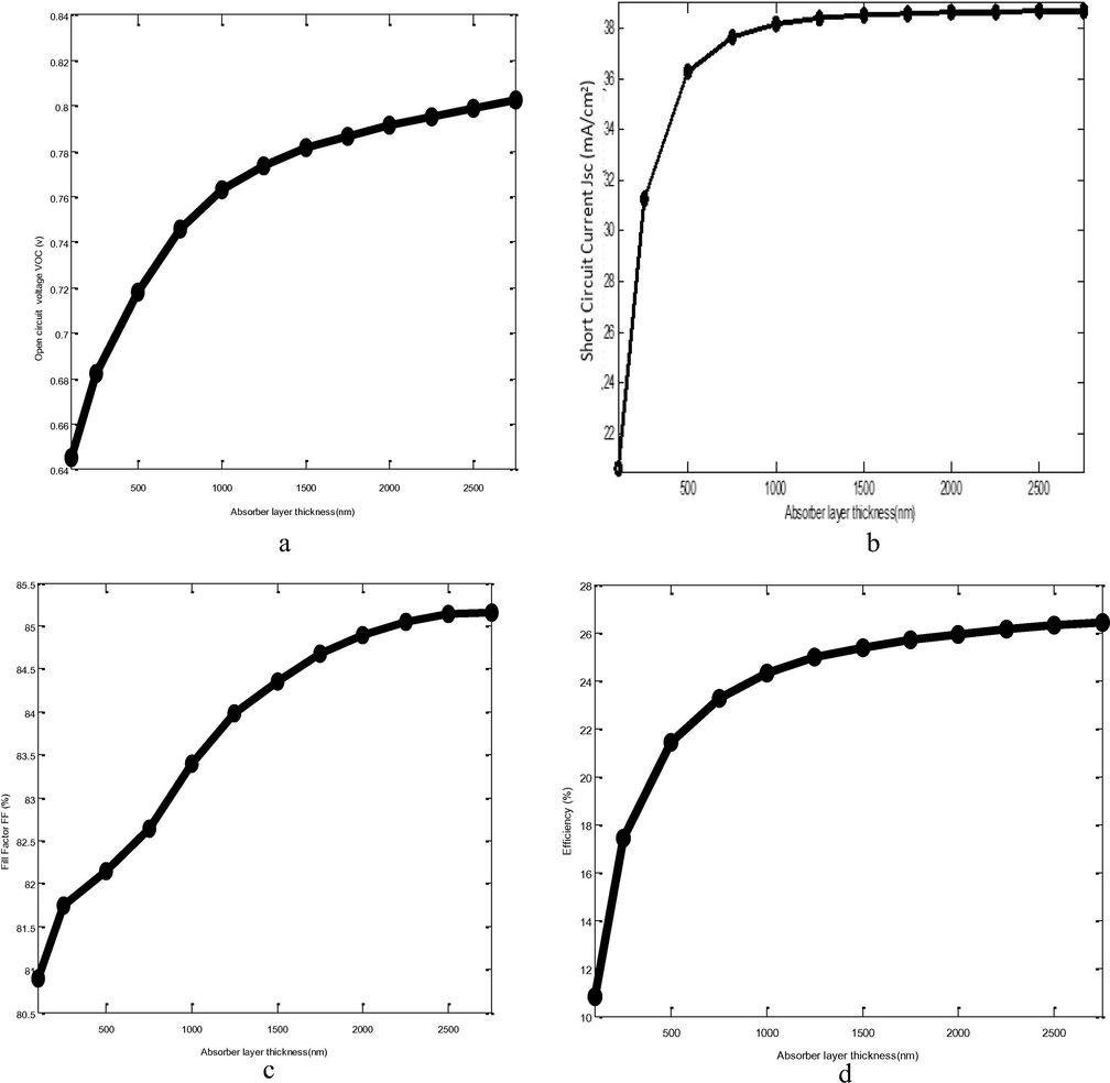
For
, all output parameters change positively. Indeed, the thicker the absorber layer is, the greater is the incidents photons quantity absorbed and the greater the conversion yield. The open circuit voltage
(Fig. 5a) continues to evolve remarkably, which allows us to record the performances recorded in Table 2.
Absorber layer thickness (nm)
500
0.7180
36.31
82.16%
21.42%
1000
0.7633
38.18
83.39%
24.31%
2500
0.7989
38.66
85.15%
26.30%
Indeed, most of these results are in good agreement with those of recent work on ultra-thins and nano-scale GIGSe based solar cells (Pogrebjak, 2011, 2012), the differences being in terms of conditions and simulation parameters.
These simultaneously good values of the conversion efficiency and the shape factor are evidence of the good quality, stability and performance of the solar structure in place.
However, these parameters reach their critical values as soon as = 2750 nm and above that value, results are not good at all due to the poor value of the fill factor (Fig. 5c), of the short-circuit current (Fig. 5b) and of the efficiency (Fig. 5d). The model of the cell proposed in this work runs optimally when it is manufactured with a maximum absorber layer thickness of 2500 nm and a minimum value of 500 nm. This makes it possible to record one of the best performances in the CIGSe-based thin films, taking into account the good value of both efficiency and fill factor.
3.5 Influence of temperature
The aim here is to define the optimal temperature zone in which our cell exhibits the best characteristics. A temperature range from −40 °C for extremely cold regions to +50 °C for extremely hot regions or will be taken. And we run calculations with the thickness of the absorber layer = 500 nm and = 2500 nm.
From Fig. 6 above, the solar device operates optimally for temperature values
. These results are globally in good agreement with those of Pogrebjak (2011).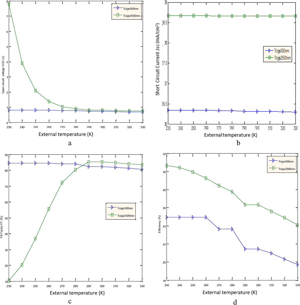
Influence of Temperature on the Output Parameters of the Cell.
4 Conclusion
This study focused on the studying of some properties of layers and interfaces for the improvement of the performances of the CIGSe solar cells using Zinc Sulfide maerial ZnS as buffer layer. The real challenge was not the use of ZnS itself, but it was to find through literature and recent work, the key values of the ZnS properties in a preferential crystallographic orientation, that allow to obtain better performances. Starting on that point, we have modeled the following cell and our simulations were ran from version 3.3 of the SCAPS-1D software. We have highlighted the benefits associated with the existence of the surface defects layer (SDL). Our buffer layer material, Zinc sulfide (ZnS), in its Blende structure, forms a more stable lattice matching with chalcopyrite structure of CIGSe. That is why most of the key values of its intrinsic properties are obtained from that orientation, especially its band gap , its electronic affinity , its dielectric constant , and later its thickness , according to simulation results. After running numerous simulations, and after judicious choice of property values of other materials we were able to retain optimum doping level for the absorber layer, and those values allow to record very promising performances in the thin films solar cells, taking into account external temperature conditions between 300 K and 330 K. Thus, a conversion efficiency of 21.42% with a fill factor of 82.15% were achieved for an absorber layer thickness of . When we increase the absorber layer thickness to , a conversion efficiency of 26.30% and a fill factor of 85.14% are simultaneously recorded. Those results are very promising given that they allow to have a value greater than about 4% compared to the previously recorded highest value (22.6%, ZSW – 2016); and they are also very pragmatic, given the feasibility of this cell device as stated above in this work. Critical values of properties such as absorber layer thickness beyond , which can indeed lead to unstable and bad device, have also been highlighted. One of the aims of this study is, first of all, to highlight the recent work that has been undertaken in this field, and going further in research, some may obtain even more interesting results by directing the work toward implementation of additional manufacturing technologies, including the use of antireflection coatings; the texturisation of the inner back layers; the use of an electron back reflector to limit recombination; the passivation of the rear and front contacts, that will allow the diffusion of sodium through the contact and even more interesting and not the cheapest one, the replacement of the usual molybdenum back contact by Gold (Au) for example, will definitely allow to obtain higher yields.
References
- Al-Ani, S.K., Ba-Yashoot, A.Kh., Makadsi, M.N., Ai-Sharbaty, A.M., 2006. Photovoltaic properties of n-(ZnS)x(CdTe)1-x/p-Si.
- Benghabrit Siham, 2015. Elaboration et caractérisation de couches minces CdS par bain chimique CBD pour application photovoltaïque. University Of Sciences and Technology of Oran, June.
- Le rôle du mécanisme de recombinaison sur les performances photovoltaïques des cellules solaires de type Cu(In, Ga)(S, Se2) Rev. Energ. Ren.: ICPWE. 2003;103–106
- [Google Scholar]
- Modelling polycrystalline semiconductor solar cells. Thin Solid Films. 2000;361–362:527-532.
- [Google Scholar]
- Cho Dae-Hyung, Lee Woo-Jung, Wi Jae-Hyung, Han Won Seok, Kim Tae Gun, Kim Jeong Won, Chung Yong-Duck, 2016. Interface analysis of Cu(In,Ga)Se2 and ZnS formed using sulfur thermal cracker. ETRI J. 38(2). http://dx.doi.org/10.4218/etrij.16.2515.0031.
- Numerical simulation of Cu(In, Ga)Se2 solar cells performances. J. Energy Power Eng.. 2015;9:1047-1055.
- [CrossRef] [Google Scholar]
- Direct evidence of a buried homojunction in Cu(In, Ga)Se2 solar cells. Appl. Phys. Lett.. 2003;82:127.
- [Google Scholar]
- Microstructural characterization of Cu-poor Cu(In,Ga)Se2 surface layer. Thin Solid Films. 2012;520:2873.
- [Google Scholar]
- Martin Green, A., Keith Emery, Yoshihiro Hishikawa, Wilhelm Warta, Ewan Dunlop, D., Dean Levi, H., Anita Ho-Baillie, W.Y., 2016. Solar cell efficiency tables (Version 49), Progress in Photovoltaics and applications. (November 2016) DOI:10.1002/pip.2855.
- Theoretical analysis of the effect of conduction band offset of window/CIS layers on performance of CIS solar cells using device simulation. Solar Energy Mater. Solar Cells. 2001;67:83.
- [Google Scholar]
- Simulation of high efficiency CIGS solar cells with SCAPS-1D software. Elsevier, Energy Procedia. 2015;74:736-744.
- [CrossRef] [Google Scholar]
- Direct evidence of Cd diffusion into Cu(In, Ga)Se2 thin films during chemical-bath deposition process of CdS films. Appl. Phys. Lett.. 1999;72:2444.
- [Google Scholar]
- XPS analysis of CdS/CuInSe2 heterojunction. Sol. Energy Mater. Sol. Cells. 1998;50:105.
- [Google Scholar]
- Simulation study of effect operating temperature and layer thickness on thin film CIGS solar cell perfomence nano-and electronic. Physics. 2011;3(3):051-058.
- [Google Scholar]
- A.D. Pogrebnjak, V.M. Beresnev, Nanocoatings Nanosystems Nanotechnologies Bentham Sci.Publ.2012,P.147.
- Large-area CIGS modules: pilot line production and new developments. Sol. Energy Mater. Sol. Cells. 2006;90:3158.
- [Google Scholar]
- Optimization of Zinc Sulfide (ZnS) electron affinity in copper Indium Sulfide (CIS) based photovoltaic cell. Chalcogenide Lett.. 2013;10(6):189-195.
- [Google Scholar]
- SurfaceLayer band widening in Cu(In, Ga)Se2 thin films. Appl. Phys. Lett.. 2003;83:4731.
- [Google Scholar]
- Chalcopyrite/defect chalcopyrite heterojunctions on the basis of CuInSe2. J. Appl. Phys.. 1993;73:2902.
- [Google Scholar]
- computational analysis of the effect of the surface defect layer (SDL) properties on Cu(In, Ga)Se2-based solar cell performances. Elsevier, J. Phys. Chem. Solids. 2014;75:688-695.
- [Google Scholar]
- Energy Environm. Focus. 2017;6:6-14.
- Excess defect at the CdS/CIGS interface solar cells. Chalcognenide Lett.. 2014;11(11):589-596.
- [Google Scholar]
- Wan Fucheng, Tang Fuli, Xue Hongtao, Lu Wenjiang, Feng Yudong, Rui Zhiyuan, 2014. Effects of defect states on the performance of CuInGaSe2 solar cells. J. Semiconductors 35 (2), DOI:10.1088/1674-4926/35/2/024011.
- Won Song, Bo-Ra Koo, Seok Eui Choi, Yong-Taeg Oh, Dong-Chan Shin, 2012. Optical and structural properties of a ZnS buffer layer fabricated with deposition temperature of RF magnetron sputtering system. Int. J. Chem., Mol., Nucl., Mater. Metall. Eng. 6 (12).