Translate this page into:
The effective carrier lifetime measurement in silicon: The conductivity modulation method
*Tel.: +966 14676375; fax: +966 14673656 uaelani@ksu.edu.sa (Ussama A.I. Elani)
-
Received: ,
Accepted: ,
This article was originally published by Elsevier and was migrated to Scientific Scholar after the change of Publisher.
Abstract
Dark, gamma-induced conductivities and conductivity modulation in silicon material will be investigated for the development of carrier lifetime measurement. The present work includes a simple method for finding the carrier lifetime variation from the measured conductivity under dark and gamma irradiation conditions. It will be concluded that an improved material evaluation in the area of semiconductors and nano-materials are expected to improve the efficiency of solar cells and other opto-electronic devices.
Keywords
Silicon material
Photovoltaic devices
Conductivity modulation measurement
Minority carrier lifetime
Semiconductors
1 Introduction
The lifetime measurement is normally used in one way or another to assess material quality. High lifetimes are indicative of good material, while low lifetimes might point to problems such as inadequate crystal growth techniques that introduce dislocations or high concentrations of impurities in the semiconductor material. Processing of various semiconductor devices can also be effectively monitored and improved by systematic lifetime measurements. Previously the study of semiconductor materials, devices and circuits, lifetime measurements were useful in gaining a better understanding of generation and recombination mechanisms. With improved fabrication technology, the focus shifted away from theoretical studies to processing-related lifetime testing. However, with the new devices such as large area power devices, metal-oxide–semiconductor MOS devices and high-efficiency solar cells, there has been a considerable interest in lifetime measurements that gives an explanation to the physical recombination processes within the device. However, the measurement of carrier lifetime in silicon wafers was studied in the past three decades. This parameter is still required to be determined accurately for new composites and nano-materials. On the other hand, the conductivity modulation could alter the distribution of charge carriers available for conduction. Thus, the excess conduction loss can occur as conductivity modulation proceeds and the forward voltage will be lowered to the steady-state value, (Moslehi, 1991; Stephens, 1996; Carsten, 2001; Zhang et al., 2001; Brown et al., 2001; Nagel et al., 1991).
The present work discusses the evaluation of carrier lifetimes based on a method developed earlier by Elani et al. (2005) and more recently by Elani (2008). It will be concluded that the conductivity modulation (conductivity changes) measurement can lead to the determination of carrier lifetime. This parameter is very important for silicon fabrication in many electronic devices such as solar cells, sensors, nuclear detectors, switches and other bipolar or opto-devices. The other benefit of the current research work lies within the improvement of the computerized in-line carrier lifetime systems, such as the microwave relaxometer and wafer lifetime tester (Telecom-STV, 2003).
2 Method of analysis
Two main methods for determining the carrier lifetime are known. The first one is intended to measure the “transient” effective lifetime by injecting the silicon material with excess charge carriers from typical external sources such as electric field, optical pulses, gamma radiation and others (Eikelboom and Burgers, 1994; Cuevas and Sinton, 1997; DiGulio et al., 1981; Stewart et al., 2001; Maekawa et al., 1995). Such sources will generate excess carriers and then the effective lifetime could be determined easily. The second method is known as the steady-state technique which requires only a fixed value of carrier generation (Sinton, 2004). If surface effects are neglected and a uniform photogeneration is assumed, the bulk carrier lifetime:
Based on the previous technique reported by Elani et al. (2005), the effective lifetime of minority carrier is then reduced to:
3 Experimental procedures and results
3.1 Samples
A number of n-type monocrystalline silicon materials is used throughout the present work. Ten wafers are taken from the same batch. These wafers were supplied from Arkansas University, USA. The silicon samples are numbered horizontally and vertically across the surface of each wafer. For example, the symbol L3S4 means sample no. 4 line 3 (i.e. line zero starts from the diameter and up for each wafer and so on). A special mask was used with opening windows with an approximate area of 4 mm × 2 mm.
3.2 Experimental technique
A Jandel in-line four-probes assembly “ILFP” is used normally for measuring the resistivity across each wafer (Jandel Ltd., UK, 2001). The sample geometry was controlled by the probes spacing. A current is passed through the outer two probes; and the potential developed across the inner two probes is measured. The ILFP technique is used here to measure the dark conductivity under dark conditions (no light or external excitation) based on Eq. (2). The induced change of gamma conductivity in silicon samples could be realized when samples are exposed to gamma rays. The radiation source was a gamma cell 220 Model no. 246 with a Cobalt-60 source containing 24,910 Curies. Low intensity gamma radiation is considered with exposure times of 1–2 h which is equivalent to nearly 6323 and 12,647 Gy irradiation doses, respectively. The conductivity modulation values are then defined as the difference between gamma conductivity and dark conductivity according to Eq. (3) and the effective lifetime was determined from Eq. (4).
3.3 Dark, gamma conductivity and conductivity modulation
As mentioned by Elani et al. (2005), it was found that the dark conductivity increases at higher injected current levels and the average change in lies between 60 and 200 cm−1 across the levels in most silicon wafers.
The uniformity of bulk resistivity is an important factor for establishing the conductivity modulation mode. For instance, by exposing the silicon wafers to gamma radiation at different doses and time levels, an increase in their conductivity are obtained, and this may be attributed to the excess charge carriers produced by gamma irradiation and this will lead to an improvement in the conductivities of nearly 2–3 times of their initial values. This result could be also explained from the fact that the conductivity modulation causes a sharp increase in the gamma-induced conductivity . In fact the conductivity modulation can be deduced from Eq. (3) and the sudden changes of against the injected current makes maximum and minimum peaks through each run of conductivity measurement.
Fig. 1 illustrates a typical example of
under certain injected current levels. For instance, in sample L1S1, the maximum peak occurs at 225
cm−1 when the injected current was nearly 25 mA, whereas the minimum peak occurs at 160
cm−1, when the current level was increased to 30 mA. This phenomena did not occur in samples located near the third line across the wafer, e.g. sample L2S5, and in this case
increases linearly as shown in Fig. 2. Similar results are also plotted in Fig. 3; but for the samples located near the edges,
will be saturated at a current level of about 50 mA, e.g. sample L3S3. The change of
is therefore a very critical for selecting samples/wafers and must be considered for future fabrication procedures.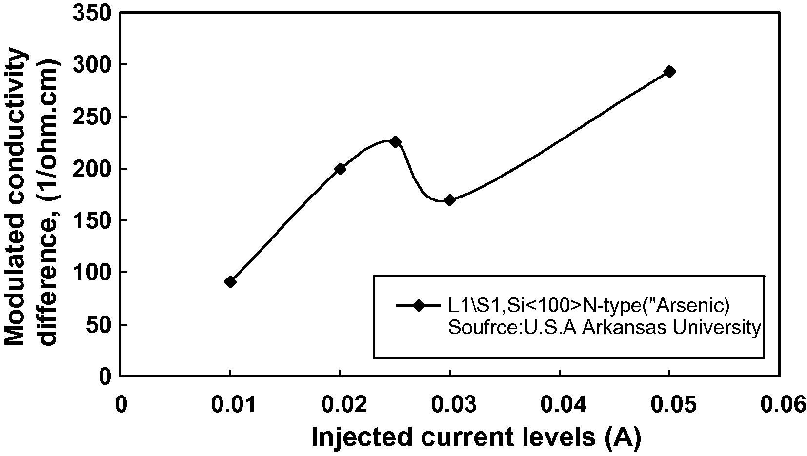
The variation of modulated conductivity differences with injected currents at the central region in Si#1 wafer.
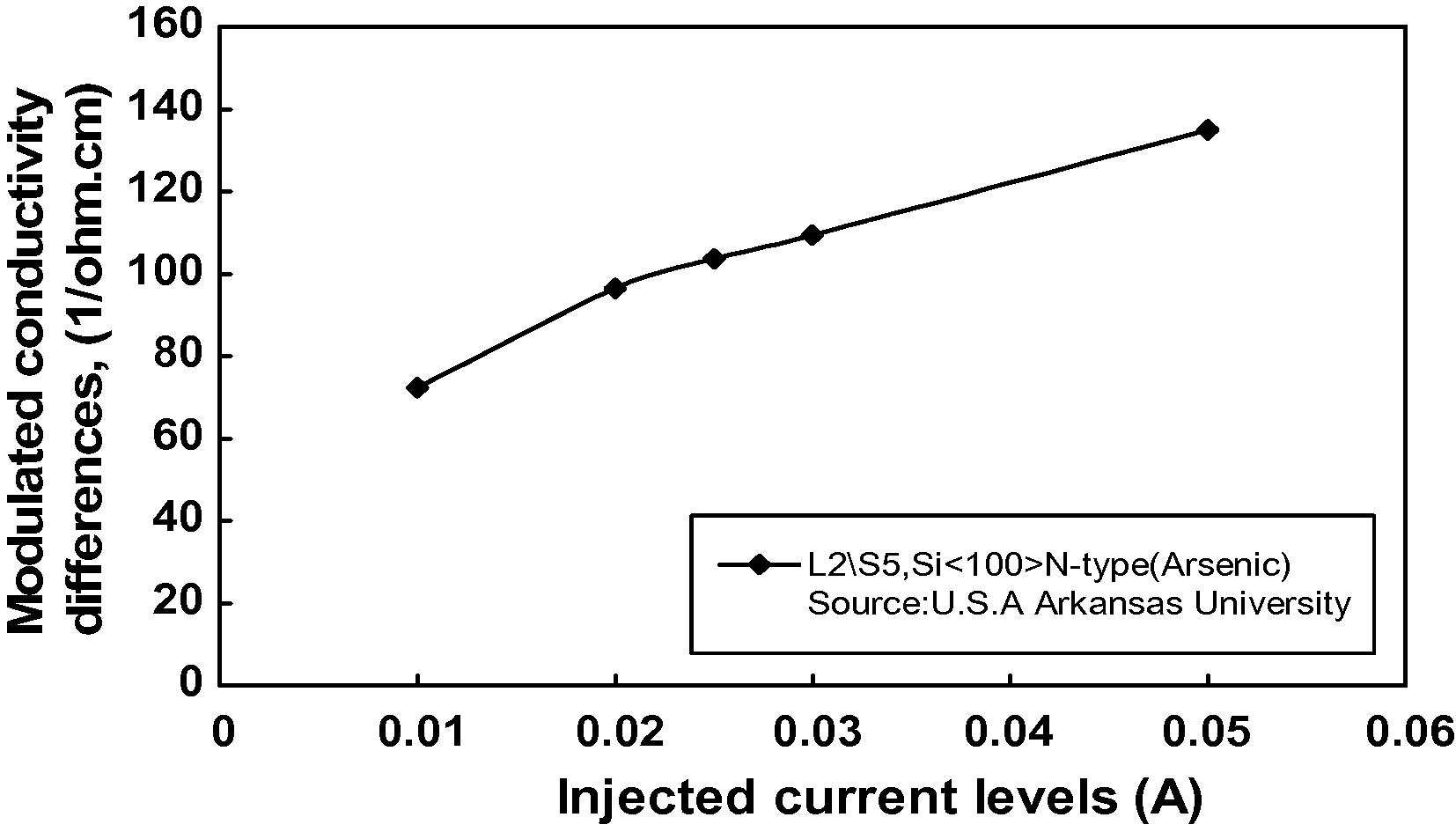
The variation of modulated conductivity differences with injected currents at the middle region in Si#1 wafer.
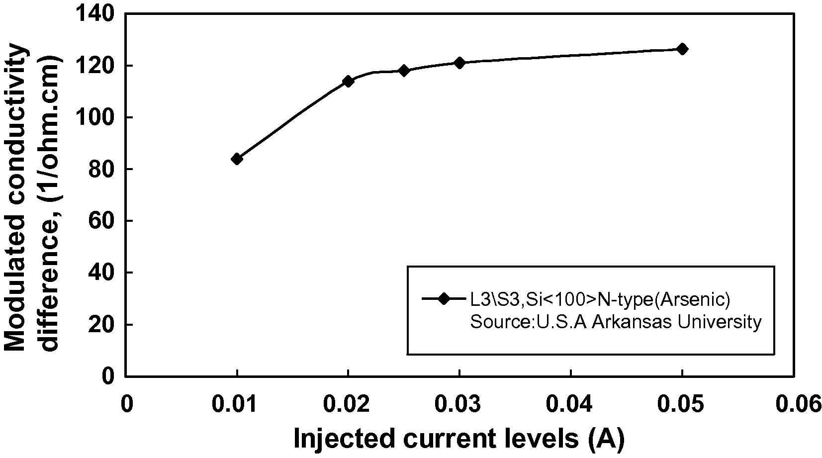
The variation of modulated conductivity differences with injected currents at the edge region in Si#1 wafer.
3.4 Carrier lifetimes determination
Based on conductivity modulation measurement, the carrier lifetime is then calculated using Eq. (4) and the results are plotted against the dark conductivity as illustrated in Fig. 4. It is clear that the lifetime is decreased as the dark conductivity increased, and this could be explained from the fact that the wafers/samples must be kept at a low injection level in order to maintain higher lifetimes (i.e. in the case of photovoltaic devices). The same experiment was repeated in a different Si wafer (e.g. p-type), but in this case it is believed that the material will resist gamma radiation more than n-type Si material and thus the lifetime is expected to be at higher levels in such materials. This case could be adopted for Si concentrated high-efficiency photovoltaic devices, space solar cells and substrate resistance modeling in Si devices/integrated circuits (Yamaguchi et al., 1996). The effect of gamma radiation on carrier lifetimes is also shown in Fig. 5.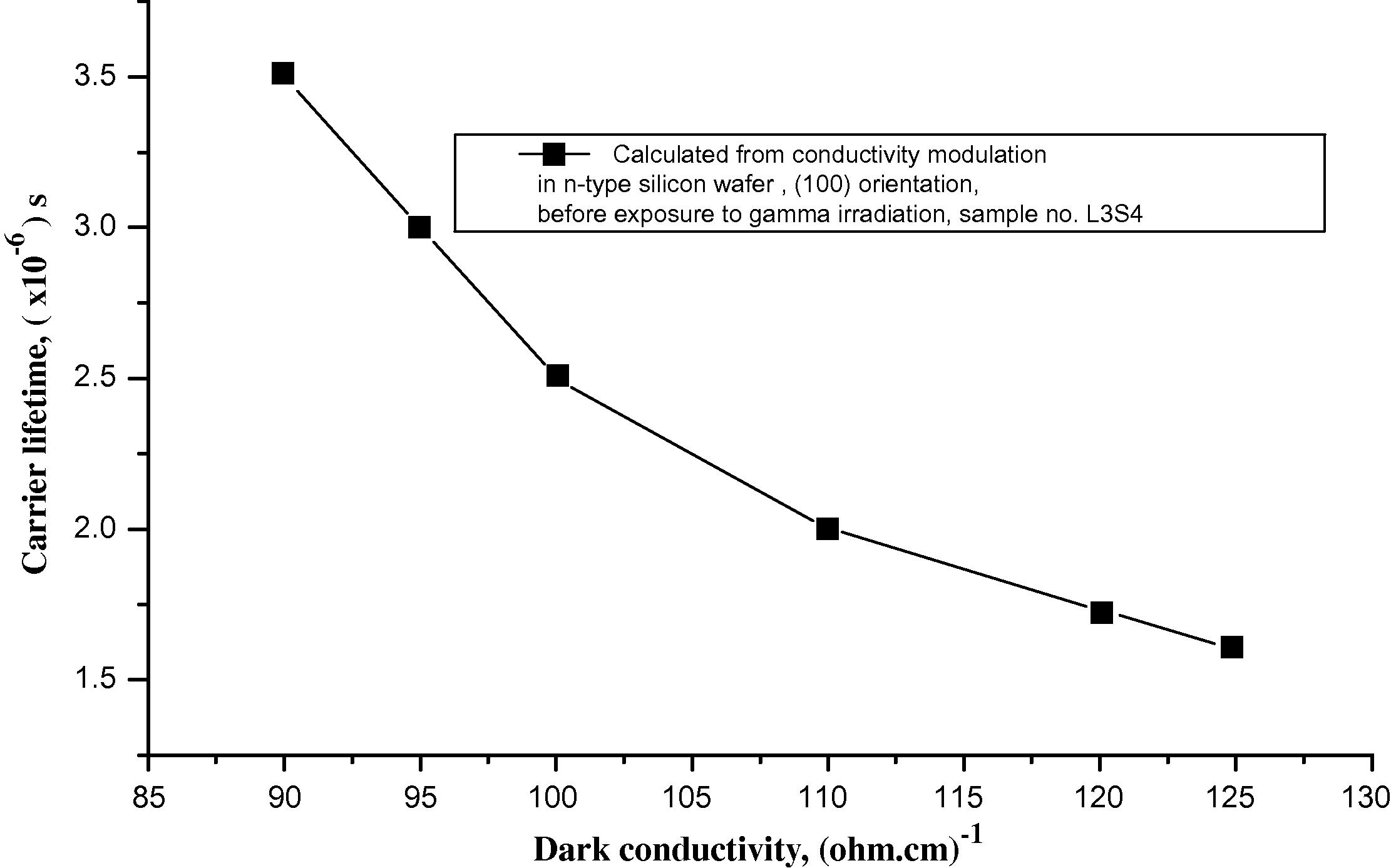
Carrier lifetime variation with dark conductivity in a silicon wafer before gamma irraddiation.
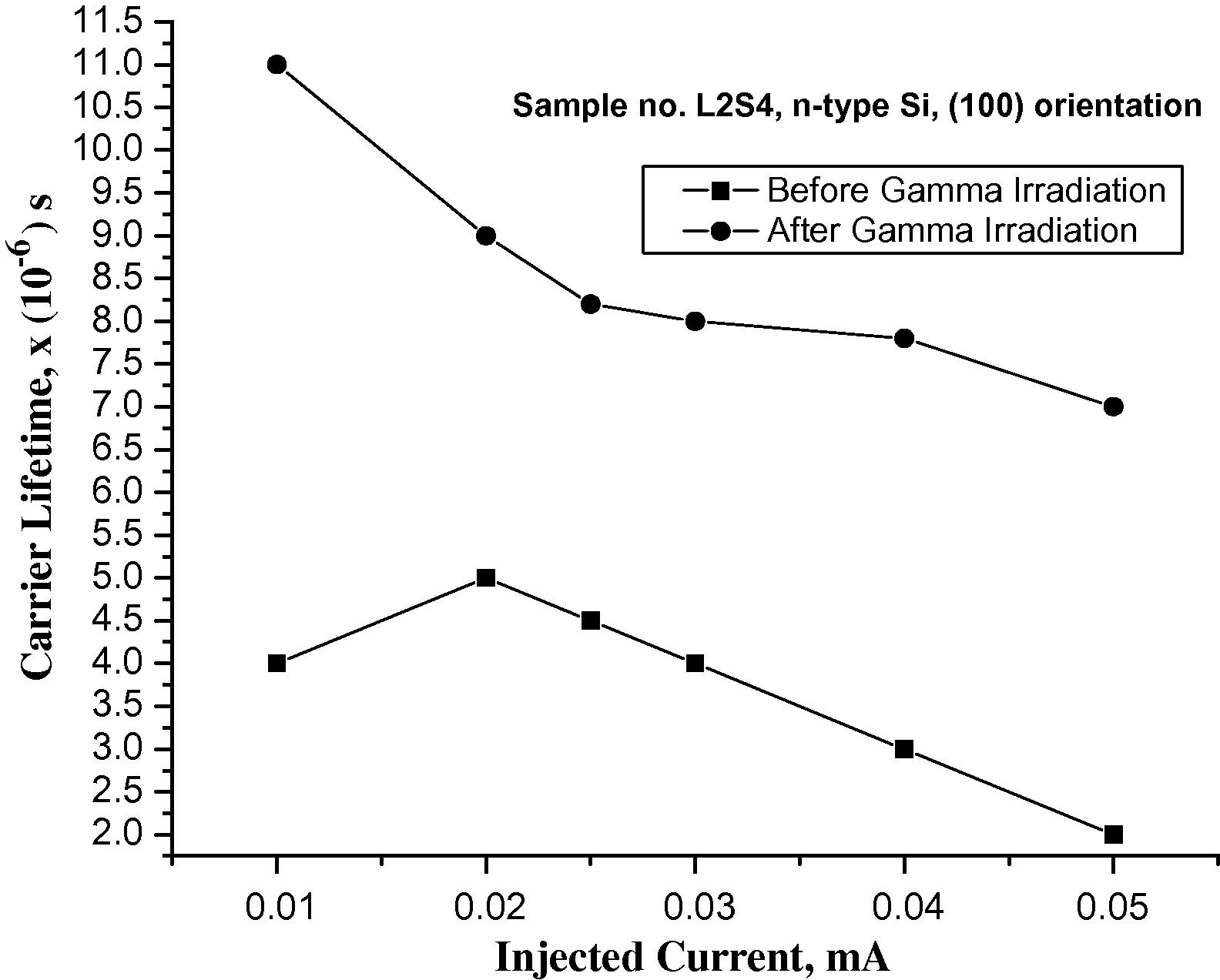
Carrier lifetime variation with injected current in silicon wafer.
It is also clear that the carrier lifetime was improved in sample L2S4 from (2.5 μs to 4.5 μs) to about (7.5 μs to 11 μs), and this may reflect that the recombination rate was reduced to its minimum. The dark and gamma irradiation lifetime measurements were repeated in order to see the effect of gamma irradiation on lifetime levels. Typical results are plotted in Figs. 6 and 7 for L1S1 and L1S2 samples, respectively.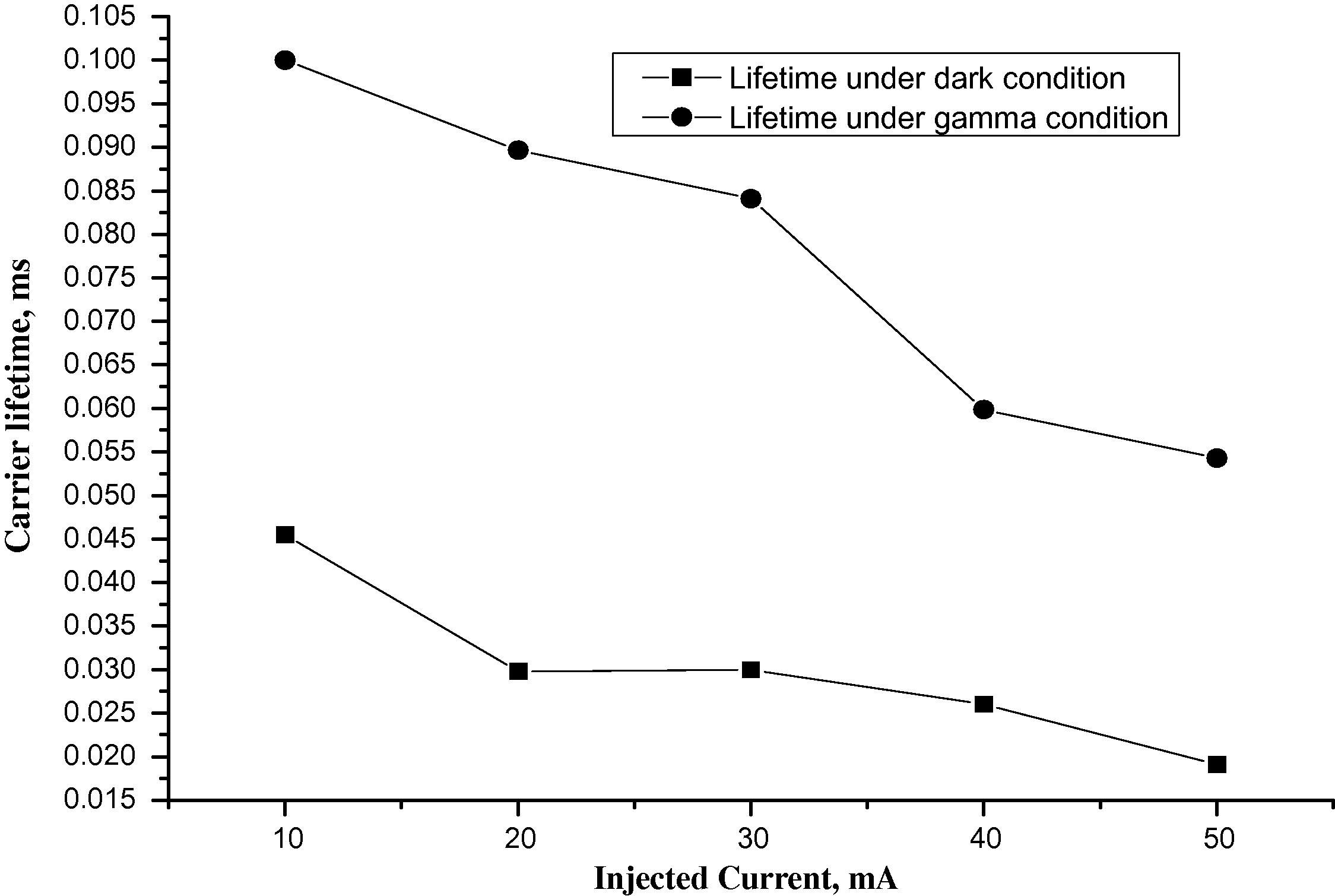
Carrier lifetime variation with injected current in silicon wafer for sample L1S1.
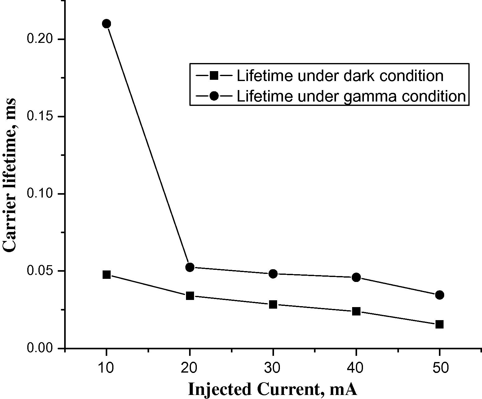
Carrier lifetime variation with injected current in silicon wafer, sample L1S2.
On the other hand, Table 1 contains more experimental results for samples numbered L2S1, L2S2, L2S3 and L2S5, respectively. These samples were taken from the same batch of silicon wafers. It is clear that the variation of carrier lifetime with injected currents has the same trend. Again, it is believed that gamma irradiation enables to establish an improvement in carrier lifetimes ratios
in the range between 1 and 6 times under various injected current levels.
Injected current I (mA)
Dark lifetime
(ms)
Gamma irradiation lifetime
(ms)
ratio
Sample no. L2S1
10
0.0434
0.1061
2.44
20
0.0265
0.0950
3.58
30
0.0224
0.0919
4.10
40
0.0197
0.0803
4.07
50
0.0129
0.0799
6.19
Sample no. L2S2
10
0.0477
0.0630
1.33
20
0.0281
0.0406
1.44
30
0.0228
0.0327
1.43
40
0.0199
0.0286
1.43
50
0.0137
0.0238
1.73
Sample no. L2S3
10
0.0477
0.0582
1.22
20
0.0289
0.0357
1.23
30
0.0253
0.0304
1.20
40
0.0229
0.0262
1.14
50
0.0156
0.0177
1.13
Sample no. L2S5
10
0.0434
0.0580
1.33
20
0.0289
0.0386
1.33
30
0.0248
0.0316
1.27
40
0.0218
0.0290
1.33
50
0.0162
0.0300
1.85
An additional important factor could be also concluded in this work for further analysis in order to extract quantitative values for a number of material parameters. These include material properties such as carrier mobilities, dielectric constants, effective masses, impurity energy levels, surface recombination velocities, diffusion lengths and saturation current densities.
4 Conclusion
Conductivity modulation method could be used as a simplified technique for determining the carrier lifetime in silicon materials. The conductivity modulation mode was measured after exposing the silicon samples to gamma irradiation; and it was found that the conductivity modulation occurred under a fixed injected current 24 mA in the silicon material. This mode is realized clearly in the central region of silicon wafers.
The carrier lifetime was also determined from conductivity modulation mode, and was almost doubled through the ratio between 1 and 6 times after exposing the silicon wafers to low-level of gamma irradiation. Higher lifetimes in the n-type silicon substrates indicate that such materials could be operated under low injection level known for sensors, nuclear detectors and complex circuits IC's. Finally, it is advised to adopt this method for evaluating other new semiconductors or nano-materials as well as for the development of a computerized unit to meet laboratory and industrial needs.
Acknowledgement
The author would like to thank the Research Centre of College of Science, King Saud University (KSU), Riyadh, Saudi Arabia for gamma measurement.
References
- Bentzen, A., Tathgar, H., Kopeak, Sinton R., Holt, A., 2005. Recombination lifetime and trap density variations in multicrystalline silicon wafers through the block. IEEE Publications, pp. 1074–1077.
- Brown, A.R., Asenov, A., Barker, J.R., Waind, P., Crees, D.E., 2001, Calibration of the numerical simulations in the design of high temperature IGBT's, p. 6. <www.elec.gla.ac.uk/dev-mod/papers/isps94/isps.html>.
- Carsten, B., 2001. The bipolar transistor is dead, longlive the bipolar transistor, p. 15. <http://www.powe-tech.com/Cartext.htm/>.
- Prediction of the open-circuit voltage of solar cells from the steady-state photoconductance. Progress in Photovoltaics: Research & Applications. 1997;5:79-90.
- [Google Scholar]
- Determination of monority-carrier lifetime in silicon solar cells from laser-transient photovoltaic effect. Journal of Applied Physics. 1981;52(12):7219-7223.
- [Google Scholar]
- Eikelboom, J.A., Burgers, A.R., 1994. Separation of bulk and surface recombination rates in silicon wafers using a new microwave reflections technique. In: 12th European Photovoltaic Solar Energy Conference, Amsterdam, pp. 1782–1783.
- The conductivity modulation of silicon samples under dark and gamma irradiation conditions. Solar Energy. 2005;78:23-29.
- [Google Scholar]
- A new method for the determination of carrier lifetime in silicon wafers and conductivity modulation measurements. Journal of Semiconductor Technology and Science. 2008;5(4):311-317.
- [Google Scholar]
- Jandel Engineering Limited, 2001. Accuracy and Precision Probes and Test Equipment, England, UK. <www.jandel.co.uk>.
- Kishimoto, N.K., 1996. Radiation-resistant photoconductivity of doped silicon under 17 MeV proton bombardment. Journal of Nuclear Materials, 1244–1248.
- Kishimoto, N., Amekura, H., Kono, K., Lee, C.G., 1998. Radiation resistance of amorphous silicon in optoelectric properties under proton bombardment. Journal of Nuclear Materials, 1908–1913.
- Contactless measurement of bulk carrier lifetime in thick silicon wafers by an induced eddy current. Semiconductor Science and Technology. 1995;10:1824.
- [Google Scholar]
- Moslehi, M.M., 1991. Semiconductor substrate minority carrier lifetime measurements. United States Patent No. 5,049,816, USA.
- Generalized analysis of quasi-steady-state and quasi-transient measurement of carrier lifetime in semiconductors. Journal of Applied Physics. 1991;86(11):6218-6221.
- [Google Scholar]
- Ravi, K.V., 1981. Imperfections and Impurities in Semiconductor Silicon. John Wiley and Sons Inc., pp. 184–200.
- Shimura, F., Huff, H.R., 1985. VLSI Silicon Material Criteria. Academic Press, pp. 191–269.
- Sinton Consulting Inc., 2006. Silicon wafer lifetime tester. www.sintonconsulting.com.
- Stephens, A.W., 1996. Application of photoconductance decay measurements to silicon solar cell characterisation. Ph.D. Thesis, The University of New South Wales, Australia.
- Sinton, R.A., 2004. Development of an in-line minority carrier lifetime monitoring tool for process control during fabrication of crystalline silicon solar cells. Annual Report, NREL/SR-520-35884, NREL National Renewable Energy Lab., Co, USA.
- Stewart, K., Cuevas, A., Macdonald, D., Williams, J., 2001. Influence of copper on the carrier lifetime of n-type and p-type silicon. 11th Workshop on Crystalline Silicon Solar Cell Materials and Processes, p. 4. <www.dspace.ann.edu.au>.
- Taylor, P.C., 2005. Characterization of amorphous silicon advanced materials and PV devices. Final Technical Report, NREL/SR-520-38678, p. 39.
- Telecom-STV, 2003. Telecom-STV Company Limited, Microwave Relaxometer Testing Equipment. <http://www.telstv.ru>.
- High-energy and high-fluence proton irradiation effects in silicon solar cells. Journal of Applied Physics. 1996;80(9):4916-4920.
- [Google Scholar]
- Electronic Properties in Materials. New York, USA: McGraw-Hill; 1963.
- Zhang, X.Y., Banerjee, K., Ameraekera, A., Gupta, V., Yu, Z., Dutton, R.W., 2001. Process and layout development substrate resistance modeling for deep sub-micron ESD protection devices. <www.ee.Stanford.edu/∼Kaustav/papers/IRS00-3pdf>.


