

Translate this page into:
Spin-resonant tunneling in ferromagnetic conductor/ semiconductor heterostructure for spin-filter application
⁎Corresponding authors. jafarali.s@vit.ac.in (S. Jafar Ali Ibrahim), aalodhayb@ksu.edu.sa (Abdullah N. Alodhayb)
-
Received: ,
Accepted: ,
This article was originally published by Elsevier and was migrated to Scientific Scholar after the change of Publisher.
Peer review under responsibility of King Saud University.
Abstract
Spin-dependent tunneling in a ferromagnetic conductor/ semiconductor is analyzed with zero external fields. The barrier transparency, dwell time, tunneling time of electrons through heterostructure and the degree of polarization efficiency are calculated in Fe/GaAs double barrier heterostructure. The polarization efficiency of Fe/GaAs and Fe/InAs double-barrier heterostructures are compared. The Fe/GaAs has a high degree spin-polarization than Fe/InAs structure. The barrier transparency peak is sharper at the high width of the barrier. The results show that the polarization efficiency is maximum when the barrier width is maximum. The tunneling lifetime of electrons is evaluated using Heisenberg’s uncertainty principle. The spin components are completely separated at high barrier width and hence can be used effectively as a spin filter.
Keywords
Ferromagnetic conductor
Barrier transparency
Resonance polarization
Spin-filter

1 Introduction
The physics of spin-polarized transport in nanoscale materials have been attracted worldwide. Research on spintronic devices such as resonant tunneling diodes, spin-based LEDs, spin-FET, and spin-transistors encourages this work (Zutic and Fabian, 2004; Datta and Das, 1990). It was shown that zero-field spin splitting is observed due to the combination of structure inversion asymmetry and bulk inversion asymmetry. After the notable work on spin-tunneling in Fe-Ge-Co, Fe-Ge-Pb and Ni-NiO-Ni, ferromagnet-based heterostructure is analyzed theoretically and experimentally (Julliere, 1975; Maekawa and Gafvert, 1982). Such junctions can be used as field sensors and non-volatile storage media (Wang et al., 2002).
Spin-dependent tunneling in ferromagnet/ insulator/ 2DEG junction, ferromagnet/ quantum dot/ ferromagnet junction, ferromagnetic/ insulator junction, ferromagnet/ insulator/ semiconductor/ insulator/ ferromagnetic junction, ferromagnet/ insulator/ superconductor junction, ferromagnetic/ ferromagnetic junction, superconductor/ferromagnet/superconductor junction, ferromagnet/ semiconductor junction, δ-doing in ferromagnet/ semiconductor junction is available in the literature (Hammar and Johnson, 2001; Ma et al., 2009; Zervos, 2003; Wolski et al., 2015; Kitamura et al., 2016; Chen et al., 2007; Lu et al., 2013; Zhang and Li, 2006; Dakhlaoui et al., 2020). Recently, spin-polarized transport in semiconductor trilayer and a triple barrier is also reported (Dakhlaoui et al., 2020; Cao et al., 2020; Cao et al., 2020; Lian Jin et al., 2010). Due to the lattice mismatch and conductivity mismatch between the ferromagnetic and semiconductor/ insulator regions, the spin injection in these heterojunctions is still challenging.
In this work, we reported the effect of Dresselhaus spin–orbit interaction (SOI) on spin-dependent tunneling in ferromagnetic conductor/ semiconductor heterostructure. The spin-dependent tunneling properties, such as spin resonances energy separation, spin-polarization efficiency, are evaluated using the transfer matrix method. The detailed procedure to form the transfer matrix in the symmetrical double-barrier heterostructure is given in section 2. The barrier transparency, tunneling lifetime of electrons and polarization efficiency are calculated for different barrier widths in Fe/GaAs heterostructures. The need for more data on spin-dependent tunneling properties, such as dwell time in this heterostructure, induces us to do this work. The spin-dependent tunneling properties are examined, and the results as well its corresponding the discussions are given in section 3, followed by the conclusion.
2 Theoretical model
According to the Stoner-Wohlfarth model, the spin-up and spin-down energy band offset in the ferromagnetic region is given by an exchanged splitting Δ (Xiao-Hua, 2009). In the ferromagnetic conductor, the effective one-electron Hamiltonian based on the simple free-electron approximation is (Bruno Chandrasekar et al., 2016)
. Here
represents the molecular field,
is the Pauli spin operator, and
represents the internal energy exchange in the ferromagnetic conductor layer.
where h0 is the one-half of the exchange splitting energy (Δ) (Wang et al., 2002). For the fixed in-plane wave vector, the eigen functions of the electrons are of the form
, where
is an in-plane coordinate of the barrier. Here ‘+’ and ‘-' correspond to an electron's spin-up and spin-down states, respectively. The electron propagations in the good region are described below:
Here
is the wave vector in the ferromagnetic layer which is spin-dependent (Wang et al., 2002);
The electron motion in the semiconductor region is (Bruno Chandrasekar et al., 2016)
where
is the conduction band mismatch between the ferromagnetic conductor and non-magnetic semiconductor and
is the Dresselhaus Hamiltonian. The Dresselhaus Hamiltonian and the corresponding diagonalization procedure are taken from the literature (Bruno Chandrasekar et al., 2016; Li and Guo, 2006). The propagation of electrons in the semiconductor region is given as,
where the wave vectors in the barrier regions are given as
According to the boundary conditions,
and
, the transfer matrix is formed. The coefficients
,
,
and
are related as
where S represents the transfer matrix. The transmission coefficient
is found, and hence the polarization efficiency is evaluated from the given formula
3 Results & discussions
The spin-dependent tunneling properties of electrons are studied in the ferromagnetic conductor/ non-magnetic semiconductor heterostructure. Fig. 1 compares the spin-polarization between Fe/GaAs and Fe/InAs double-barrier heterostructures. In the Fe/GaAs heterostructure, the parameters used in the calculations are
;
; Δ = 3.46 eV;
eV;
and in the Fe/InAs heterostructure, the parameters used in the calculations are
;
; Δ = 3.46 eV;
eV;
(Xiao-Hua, 2009). From the figure, it is seen that the spin-polarization efficiency is higher in Fe/GaAs heterostructure than in Fe/InAs heterostructure.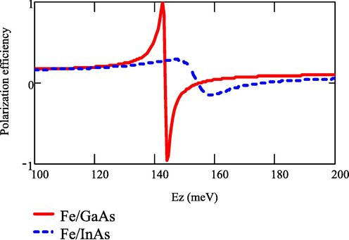
Polarization efficiency for Fe/ GaAs and Fe/ InAs heterostructures.
Fig. 2 shows the spin-polarization efficiency and barrier transparency for various barrier widths in Fe/GaAs double barrier heterostructure. When the barrier width of the heterostructure is 30 ang, the polarization efficiency is maximum but not 100 %.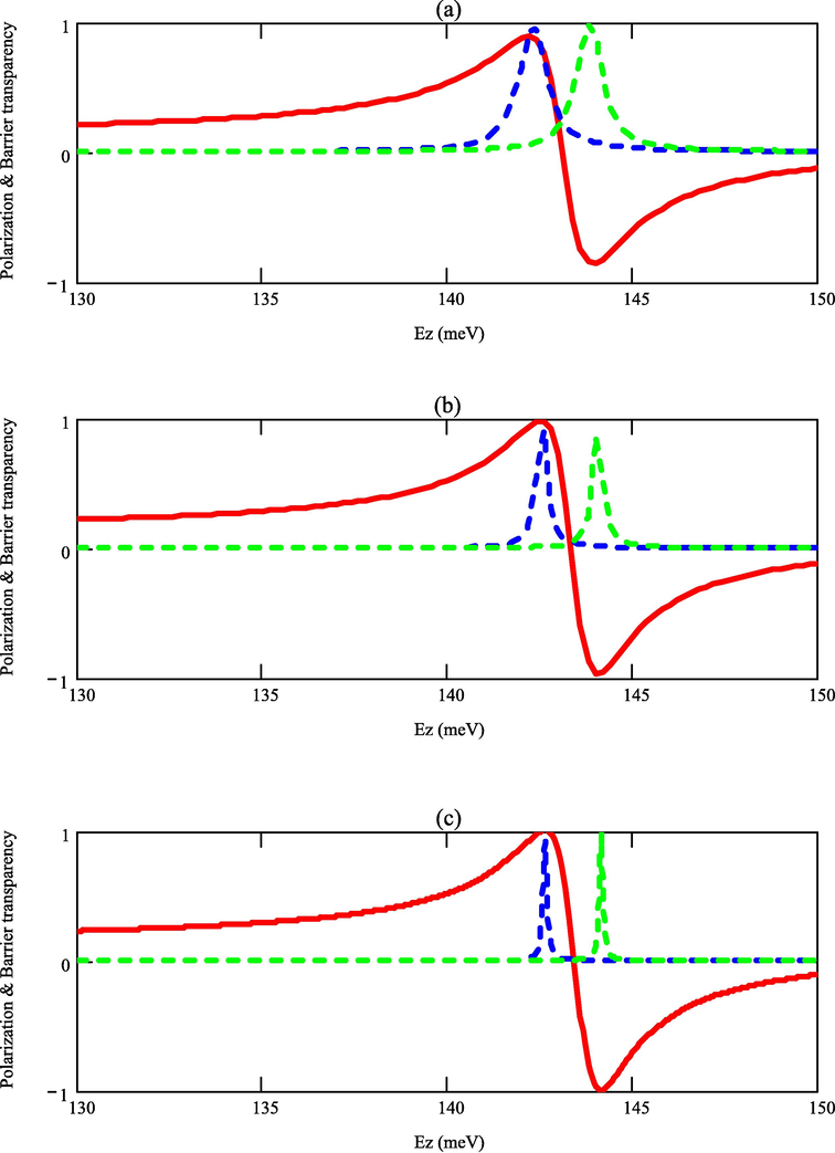
Polarization efficiency & barrier transparency for various barrier widths (a) 30 ang, (b) 35 ang, and (c) 40 ang.
The barrier width is more than 30 ang, so one can reach 100% polarization efficiency in this heterostructure. Hence by increasing the width of the semiconductor, one can obtain the maximum polarization though the barrier width changes and the energy of resonance polarization remains the same. The width of the barrier transparency depends on the barrier width. The width of the barrier transparency peak decreases as the barrier width increases.
The variation of the full width at half maximum of the barrier transparency peak is graphically shown in Fig. 3. The separation between the spin-up and spin-down resonances on the energy scale is 1.5 meV, independent of barrier width.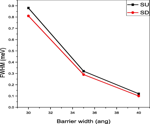
Full width at half maximum for various barrier widths.
To understand the spin-dependent tunneling properties clearly, spin-up and spin-down electrons' dwell time and tunneling lifetime are evaluated as a function of barrier width. Heisenberg's uncertainty principle is used to find the tunneling time of electrons. The width of the transparency peak for spin-up and spin-down resonances are different; hence, the tunneling times of spin-up and spin-down are also different. The spin-down electrons take more time in the heterostructure than the spin-up electrons. When the barrier width is 30 ang, the tunneling lifetime of spin-up electrons is 0.7498 ps, and the tunneling lifetime of spin-down electrons is 0.8146 ps. The same is 5.4986 ps and 6.5983 ps, respectively, when the barrier width is 40 ang. Hence the tunneling lifetime depends on the nature of spin, and barrier width, whereas the spin separation is independent of barrier width. The calculated tunneling lifetime is shown in Fig. 4. Since no data is available to compare these results, which need further theoretical analysis.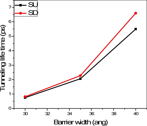
Tunneling lifetime for various barrier widths.
The dwell time of the incident electrons in the heterostructure is given as (Li and Guo, 2006)
Like tunneling lifetime, dwell time is also high for spin-down electrons than spin-up electrons. The dwell time is 10-13 s when the barrier width is 30 ang, and the same is 10-12 s when the barrier width is 40 s. The observed dwell time of electrons is graphically shown in Fig. 5. Hence by varying the width of the ferromagnetic conductor in this heterostructure, one can tune the polarization efficiency, the width of the barrier transparency peak, the tunneling lifetime and the dwell time of the electrons.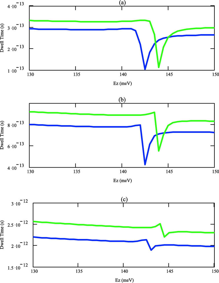
Dwell time for various barrier widths (a) 30 ang, (b) 35 ang, and (c) 40 ang.
Fig. 6 shows the barrier transparency of electrons in Fe/GaAs heterostructure with a barrier width of 60 ang. The transparency peaks are mono-energetic in nature. This is clear evidence that the different orientations of spins are separated in terms of energy. Hence, using this heterostructure, one can separate the electrons based on spin. An effective spin filter can be constructed with this heterostructure with these parameters.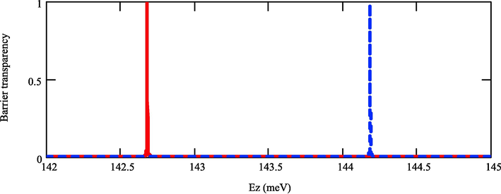
Barrier transparency in Fe/GaAs.
This work can be extended to study the electron spin transport in the same heterostructure with external electric and magnetic fields. Moreover, one can study the tunneling of the light hole and heavy hole in this heterostructure.
4 Conclusion
The transfer matrix method is employed to find the barrier transparency, spin separation, and polarization efficiency in the Fe/GaAs symmetrical double-barrier heterostructure. Higher polarization efficiency is obtained in Fe/GaAs heterostructure than in the Fe/InAs structure. High barrier width enhances polarization efficiency. The tunneling lifetime of electrons is greater when the barrier width is high. The dwell time of electrons increases in unit order as the width increases from 30 ang to 40 ang. Using this heterostructure, a spin filter is proposed. Our simulation results presented herein show that we can achieve a higher polarization efficiency by using heterostructures having larger barrier width. These results bring much more interesting phenomena in the basic science of electron transport in the heterostructure in the future. Our simulation studies and finding are promising, and it can be useful to the scientific communities working in this domain in planning their fabrication and experiments.
Acknowledgment
The authors extend their appreciation to the Deputyship for Research and Innovation, Ministry of Education in Saudi Arabia for funding this research work through the project no. (IFKSUOR3-099-3).
Declaration of Competing Interest
The authors declare that they have no known competing financial interests or personal relationships that could have appeared to influence the work reported in this paper.
References
- Effect of Barrier Width on Spin-Dependent Tunneling in Asymmetrical Double Barrier Semiconductor Heterostructures. J. Nanoengg. Nanomanu.. 2016;6:175.
- [CrossRef] [Google Scholar]
- Effect of 'Al' concentration on spin-dependent resonant tunneling in InAs/Ga1−y Al y As symmetrical double-barrier heterostructures. Bull. Mater. Sci.. 2016;39:1435-1440.
- [CrossRef] [Google Scholar]
- Rashba spin-orbit coupling induced electron-spin polarization in a realistic 3-layered semiconductor heterostructure. Superlattice. Microstruc.. 2020;143:106545
- [CrossRef] [Google Scholar]
- Dresselhaus spin-orbit coupling induced electron-spin polarization in a 3-layered semiconductor heterostructure. J. Mag. Mag. Mat.. 2020;513:167217
- [CrossRef] [Google Scholar]
- Oscillations of tunnel magnetoresistance induced by spin-wave excitations in ferromagnet-ferromagnet-ferromagnet double-barrier tunnel junctions. Phys. Rev. B. 2007;76(14):144409
- [CrossRef] [Google Scholar]
- Elmobkey, Shaffa Almansour, Ibtessam Alnaim, Spin-polarized transmission across heterostructure based on an InAs/GaSb/InGaAs system: Effect of accelerating quantum wells Che. Phy. Lett.. 2020;757:137866
- [CrossRef] [Google Scholar]
- Alanoud Al Suwaidan, Hadeel Elmobkey, Shaffa Almansour, Ibtessam Alnaim, Magnetic field effect on spin-polarized transport in asymmetric multibarrier based on InAs/GaAs/GaSbsystems. Phys. B. 2020;597:412403
- [CrossRef] [Google Scholar]
- Electronic analog of the electro-optic modulator. Appl. Phys. Lett.. 1990;56(7):665.
- [CrossRef] [Google Scholar]
- Spin-dependent current transmission across a ferromagnet–insulator– two-dimensional electron gas junction. Appl. Phys. Lett.. 2001;79:2591.
- [CrossRef] [Google Scholar]
- Tunneling between ferromagnetic films. Phys. Lett. A. 1975;54(3):225-226.
- [CrossRef] [Google Scholar]
- Nonequilibrium Effect in Ferromagnet-Insulator-Superconductor Tunneling Junction Currents. W. J. Cond. Matt. Phys.. 2016;6:169.
- [CrossRef] [Google Scholar]
- Dresselhaus spin-orbit coupling effect on dwell time of electrons tunneling through double-barrier structures. Phys. Rev. B. 2006;73:205311
- [CrossRef] [Google Scholar]
- Effect of Rashba spin-orbit coupling on the spin-dependent transport in magnetic tunnel junctions with semiconductor interlayers. J. Appl. Phys.. 2010;107:103722
- [CrossRef] [Google Scholar]
- Controllable electron-spin polarization by δ-doping in a hybrid ferromagnet and semiconductor nanostructure, Euro. Phys. Lett.. 2013;101(4):47001.
- [CrossRef] [Google Scholar]
- Spin-polarized transport in an asymmetric ferromagnetic/quantum dot/ferromagnetic system. J. Appl. Phys.. 2009;105:07c912.
- [CrossRef] [Google Scholar]
- Electron tunneling between ferromagnetic films. IEEE Trans. Magn.. 1982;18(2):707-708.
- [CrossRef] [Google Scholar]
- Tunneling time of spin-polarized electrons in ferromagnet/insulator (semiconductor) double junctions under an applied electric field. J. Appl. Phys.. 2002;91:1318.
- [CrossRef] [Google Scholar]
- Spin and charge transport in double-junction Fe/MgO/GaAs/MgO/Fe heterostructures. J. Appl. Phys... 2015;117:043908
- [CrossRef] [Google Scholar]
- A Xing-Tao, Liu Jian-Jun, The influence of the Dresselhaus spin–orbit coupling on the tunneling magnetoresistance in ferromagnet/insulator/semiconductor/insulator/ferromagnet tunnel junctions. Chin. Phys. Lett. B. 2009;18:749.
- [CrossRef] [Google Scholar]
- Investigation of spin-polarized resonant tunneling through double-barrier magnetic tunnel junctions by the self-consistent solution of the Poisson-Schrödinger equations. J. Appl. Phys.. 2003;94:1776.
- [CrossRef] [Google Scholar]
- Rashba spin-orbit effect on spin-tunneling time in a ferromagnetic∕ semiconductor∕ ferromagnetic heterojunction with a tunnel barrier. J. Appl. Phys.. 2006;99(1):013907
- [CrossRef] [Google Scholar]
- S, Das Sarma, Spintronics: Fundamentals and applications. Rev. Mod. Phys.. 2004;76(2):323-410.
- [CrossRef] [Google Scholar]