

Translate this page into:
Simulation-based design of 1-D copper nanograting device for sensing application by studying electromagnetic properties on Cu/Air interface
⁎Corresponding author. zainashfaq147@gmail.com (Zain Ashfaq)
-
Received: ,
Accepted: ,
This article was originally published by Elsevier and was migrated to Scientific Scholar after the change of Publisher.
Abstract
Sensing devices has been an interesting area of study because of their immense application in practical life. In the present work, the extraordinary optical transmission (EOT) along with surface plasmon polaritons (SPPs) excitation at the metal/ dielectric interface is investigated RF-module of COMSOL Multiphysics 5.3a has been used to investigate copper (Cu) nanograting structure on the glass substrate in periodic arrangement of 1-dimensional (1D). The visible-infrared electromagnetic wavelength of 400–900 nm has been used to excite the SPPs at the interface and a light port is provided from the substrate side. The optimum EOT has been investigated at transmission spectra of 0th order. During this process thickness of the slit is fixed at 50 nm, the periodicity of the unit cell is fixed at 700 nm, and the width of the slit changed to check its effect on the EOT. Additionally, phenomena of near field investigation have also used to explore the transmission-based performance of field at the specific boundary of copper (Cu) and air which confirm spectra outcomes of transmission thorough the fabricated device. The optimum value of EOT found when the width of slit is at 250 nm for the Cu/air interface. The device used for this purpose is modeled in COMSOL. Along the EOT the SPPs phenomena is also investigated by using present modeled device. These phenomena are observed by studying the electric and magnetic parts of the device that models the Cu/Air interface. We tested it with different slit widths ranging from 50-450 nm. The coupling efficiency and sensitivity of Cu/Air 1D device design at optimum slit width of 250 nm calculated. Such devices are increasingly applicable in bio photonics sensing of DNA structure, in vivo study of the internal structure of the body, imaging, surface chemical reaction, environmental remediation, and in various solar cell industries (plasmonic solar cell).
Keywords
Sensors
Surface plasmon polaritons (SPPs)
Grating Coupling
Photolithography Enhanced Optical Transmission (EOT)
Surface Plasmons (SPs)

1 Introduction
Plasmonic Based devices has got attention of the researchers in last few decades due to their enormous applications in unique sensing and optical applications(Divya, Selvendran, Raja, & Sivasubramanian, 2022; Garcia-Vidal et al., 2022; Wang et al., 2022; Zhao, Xue, Ji, Li, & Li, 2021).When light passes through something smaller than its wavelength, its transmission changes in accordance (λ /r)2 as discussed by Bethe in 1944. In simple words, λ represents the length of a wave, and r represents the size of the opening (Bethe, 1944). When light shines on a patterned structure, it creates two types of light modes: from this one that is scattered far from where the light meets the material and another that only exists at that meeting point. When the wave vector of the incident light increases, the momenta of the light, combined with the momenta of the oscillating free electrons at the metal's surface, also increase (Jia et al., 2023) and creates SPPs. Surface plasmon resonance (SPR) occurs at the interface when the momenta of electrons and light that hits a material are matched with each other. When the light goes through a very small slit, it scatters, and this makes the light brighter. This is called enhanced transmission of light or enhanced optical transmission. Optical transmission is improved by factors such as the type of light, the shape, and the material properties of the metal. These special structures can be used for many things like sensing biological substances quickly, as well as making detailed patterns on surfaces using light (Ashfaq et al., 2023; Iqbal et al., 2020; Li et al., 2020). Different ways of understanding how light interacts with small structures have been reported (Obalalu et al., 2023) for instance one could able to use the transfer matrix method and mathematical calculations have been analyzed and understand the (Daneshvar et al., 2021; Galal et al., 2024; Kaushik, Singh, & Devi, 2023; Park, Yu, Park, & Park, 2023) In phase groove transmission mode, cavity mode groove and slit wavelength mode are three ways reported to improve the EOT(Chu et al., 2020; Daneshvar et al., 2021). Another phenomena of nanohole array to improve the EOT reported by Zhiquan Chen (Alam et al., 2023; Chen et al., 2019). Researchers group has measured the nanosphere's 46 % optimum sensing capability in respect of its optimum EOT and nano cylindrical shape is 56 %. The thickness effects on EOT unit cell has been investigated by Evan S. H. Kang et al (Kang, Ekinge, & Jonsson, 2019).
Many of the previous modeling designs had been studied for different applications by using the 1D grating of Gold (Au)/ Air interface and by using 1D grating of silver Ag/Air interface(Wei, Choy, Chen, & Chew, 2011; Zhou et al., 2019). Although Au/Air interface designed device is more efficient but Au is expensive as compared to Cu and Ag. Ag/ Air interface is low cost but not more efficient as compared to Au and Cu (Nigoghossian et al., 2015).
Considering that other metals are very expensive and already reported in literature in the present work copper Cu used as novel metal to explore the unique characteristics for application in sensing device. Reporting the nano grating of Cu 1D structure device is economical as compared to gold (Au) and silver (Ag) as the gold share price at this time in market 1940$, silver rate 24$ and copper rate 4$.So, in this study, it is worth mentioning that a new metallic rectangular grating of Cu used for 1D grating Cu/Air interface designed has been studied which is a novel grating used to study different plasmonic applications. The motivation of using Cu metal for interference is good conductivity, being reported first time for sensing application, cost effective and easily availability. This study shows that light can pass through a special type of pattern made of tiny copper structures The COMSOL Multiphysics 5. 3a software has been used to simulate the nanograting of Cu. The thickness of 50 nm and grating of Cu repeating pattern every 700 nm has been placed on top of a glass substrate. The optimum value of EOT is also calculated by changing the nanograting slit width from 50 to 450 nm. The electric and magnetic field components measured during this process as well to verify the optimum value of slit width. The coupling efficiency and sensitivity were also calculated.
2 Validity of model
The validity of the model has been checked by comparing simulation data with Fresnel equations for Transmission (T) and Reflection (R) through the glass to air (Shih et al., 2015; Shurcliff, 1974)
In the simulation design only air and galss is used in the subdomains. Then light falls on the modeled design for the analysis of geometry. The transmission and reflection value has been calculated by using finite element analysis (FEA) method and plot process verify that air n1 = 1 and glass n2 = 1.5 then T = .96 and R = .04 as shown in Fig. 1. Putting the values of n1 and n2 into equations (1) and (2) has the same results. So present design model and Fresnel equations results show the same results. Hence the model works properly at 100 % accuracy.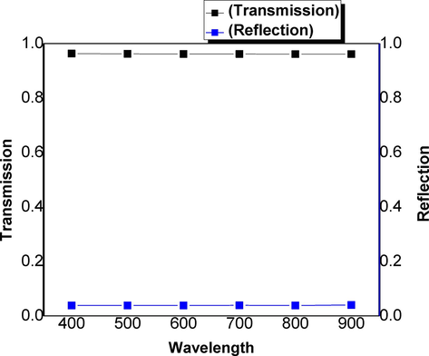
Simulation data of Reflection and Transmission obtained from the designed model to check the validity of the present model.
3 Theory and numerical modeling
An electromagnetic wave can cause a substance to become polarized. This can provide information about the substance's physical properties, such as how well it conducts electricity and its ability to store electric charges and magnetic fields. Simply put, these properties explain the charges and currents found in a substance using equations created by Maxwell.
The Cu used for this purpose because it’s also verified the condition of Surface Plasmon Polaritons formation which is its real part of relative permittivity is negative and greater than the imaginary part of relative permittivity and verified the equation (3).
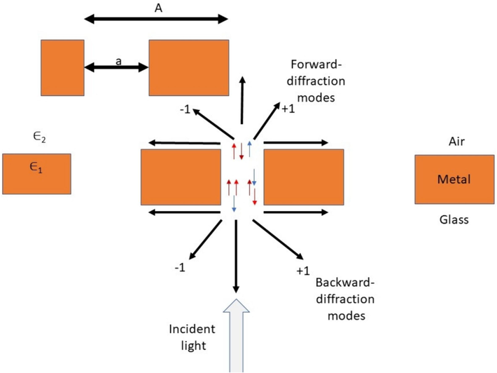
Shows the effect of p and s polarization incident light component on various diffraction modes.
The formation of SSPs occurs by the incident light p polarization component on the nanograting of the Cu/Air interface which results in the coupling of incident light with surface plasmon at the surface. The mathematical relation for this phenomenon can be expressed as
Kx = ko + N = Kspp (4)
In this equation, / A denoted the grating vector and the delta is 0 for s-polarized and 1 for p-polarized light.
The model used in this work has been created by using the COMSOL RF module. The model designed has been shown in Fig. 3, including all the ports, subdomains, boundary and other conditions used for the present study. There are seven subdomains two are glass substrate, three air, and two metals of Cu. All subdomains are set along both sides with periodic boundary conditions (PBC). The light is incident from the glass substrate which act as the excitation port.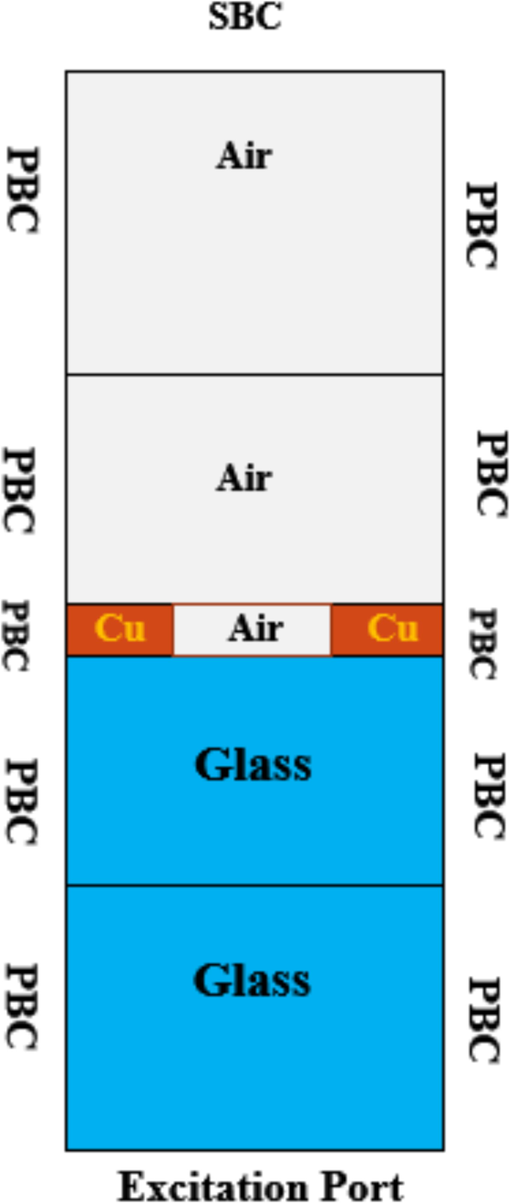
The modeled unit cell has different parts and conditions at its edges. It is 50 nm thick and repeats every 700 nm.
The model was made to match the real-life device as their periodicity lies in the visible region. So, in this present work a pattern of Cu nanograting has been used that repeats every 700 nm. The 50 nm thick slit has been used which is optimum value to couple the air/Cu moment at the interface. These dimensions have been selected for this study because Tahir et al already calculated this dimension are optimum for Au. To save on computer processing power, periodic condition of boundary equipped with unit cell. To gather light, exit port has been set with boundary conditions that cause scattering. To make the models work well, we used a mesh with small triangular shapes that are 20 nm in size, like the ones in Fig. 4. The input has been hit by TM light at a straight angle to efficiently connect SPs at the interface of Cu and air. Recently, Tariq et al and francioso et al has reported modelling methodology by using COMSOL Multiphysics for plasmonic based study (Arshad et al., 2023; Saison-Francioso, Lévêque, & Akjouj, 2020; Tariq, Fakhri, Salim, Hashim, & Alsultany, 2022).
This picture shows how a model of a 1D Cu/Air grating is divided into small sections, with a thickness of 50 nm and a repeating pattern every 700 nm. The meshing of the model was created using COMSOL.
4 Result and discussion
This method helps to connect SPP with the light that comes in at the Cu/air surface in a good way. After shining light on the model from the bottom, the transmission spectrum was obtained by looking at how the light interacts with the grating, as shown in Fig. 5. We know that only one type of light called p-polarized light can create something called SPPs. So, the other type of light called s-polarized light is not useful for creating SPPs. Electromagnetic waves interact with metal electrons causing both positive (constructive) and negative (destructive) effects. These effects lead to the highest points called maxima R2 and the lowest points called minima R1. The peak R2 is in charge of the end of transmission and represents maxima (Iqbal et al., 2019) So these values are studied for additional calculations.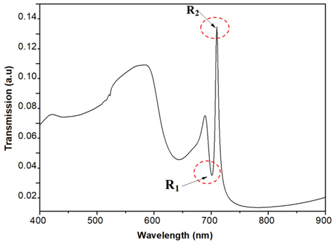
The figure shows the spectrum of light that is transmitted through a thin device called a grating. The device has a thickness of 50 nm and is made up of a pattern that repeats every 700 nm.
This figure shows the periodicity of 700 nm excited under the p-polarized component of light.
To calculate EOT, different models with varying slit widths were studied using TE and TM light. When light component of TE interacts with SPs, then it creates SPPs along the interface of Cu and air. This phenomenon verified by observing concavity R1 in diagram 5 below. Relation how well information is transmitted aimed at TE as compared TM for the EOT shown in Fig. 6 with a width of slit range varies from 50 nm to 450 nm. It’s important to note the highest EOT measurement recorded when the width of slit is changed from two- third to one-half of periodicity (Arshad et al., 2022; Jelich, Zhao, Chen, & Marburg, 2022; Roudsari, Pakarinen, Reischl, & Vehkamäki, 2022; Yu, Lu, Cheng, & Zhu, 2020). Because of the fundamental plasmonic in this range occurs which is eminent at the scientific works. The reason why the maximum amount of light is blocked in this particular area with small slits is that the light scatters less (Koev, Agrawal, Lezec, & Aksyuk, 2012) in proportion to a higher width of slit, this scatters light less and has low efficiency aimed at SP and incident light coupling at the interface of metal/ dielectric. Firstly, due the direct scattering transmission rate of light remains high(Koev et al., 2012). In simple terms, when using devices with a one-dimensional grating, a smaller slit width allows for the modes of plasmonic optimum to exist at the interface between copper and air. This is because there are more Fourier components present. As a result, the efficiency of the most basic plasmonic mode (0th-order fundamental plasmonic) becomes very strong. However, when the slit width is increased, the higher plasmonic modes no longer exist in the grating devices (Chang, Lin, Lee, & Huang, 2023; Guerrero-Becerra et al., 2021; Kim & Hyun, 2023; Liang et al., 2021).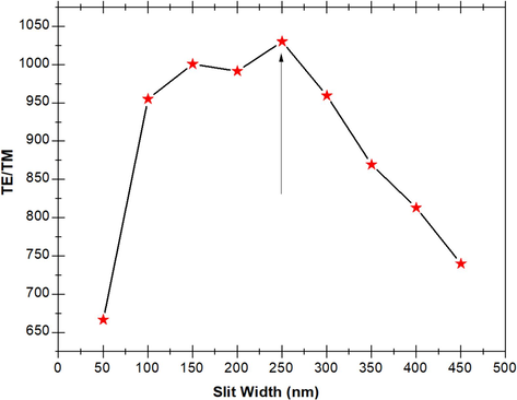
The EOT plot was calculated using different slit widths. The TE calculations were done using the values from R1 and R2 shown in Fig. 5.
To see how the field has improved, COMSOL software has been used. Electromagnetic fields on surface where copper and air meet have been much stronger for the slit width of 250 nm, as shown in Figs. 7 and 8. The models clearly show that when surface plasmons interact with electromagnetic radiation, they trigger the excitement of SPPs and amplify the field at the interface, confirming Equation 4. The coupling efficiency achieved by using the Cu/Air interface has achieved 90 % for 250 nm nanograting of 1D design as shown in Fig. 7.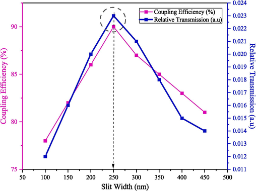
Shows the Coupling efficiency and corresponding transmission with variation in slit width from 100 nm-450 nm.
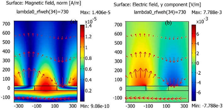
The visualization of (a) magnetic (b) electric field enhancement is seen on the The area where copper and air meet.
In a plasmonic sensor, sensitivity (S) refers to how much the wavelength (Δλ) changes compared to the change in refractive index (Δn). This sensitivity value shows how much the plasmonic sensor's resonant wavelength changes when the refractive index of the surrounding medium changes. A plasmonic sensor uses light to interact with surface plasmons on a metal surface. This interaction usually happens when surface plasmon resonances are excited. When there are substances like molecules or ions around a metal surface, the way light behaves changes. This causes the wavelength of light to shift. This change is what determines how sensitive something is. Fig. 5 also illustrates the formation of SPPs at surface and resonance wavelength observed at 700 nm R1 and R2 730 nm for the 250 nm thickness. This shows 30 nm wavelength shift in the above design model. The Cu has a refractive index at 700 nm is 0.2110 and for 730 nm has refractive index 0.22485(Johnson & Christy, 1972). The change in refractive index calculated 0.01385. By using the formula of sensitivity Here represents wavelength shift and change in refractive index. So, sensitivity calculated is 2166.06.
This picture of the model was taken with a 250 nm slit width, which is when the maximum EOT occurs.
Spectra of the transmission was found by studying figure number 6 and Fig. 8 shows the Far-field and near-field analysis was used to investigate the present 1D design of Cu nanograting device when light of wavelength visible-near infrared passes through a material with fixed thickness of 50 nm, periodicity 700 nm and variation in slit width from 50-450 nm. With the excitation of SPPs, the fields of magnetic and electric on interface of the air and Cu become stronger at 250 nm. This is important to check the transmission results which are shown in Fig. 7 along coupling efficiency.
Fig. 9 shows that the E-field and B-field values are highest when the width of slit is approached at the value of 250 nm.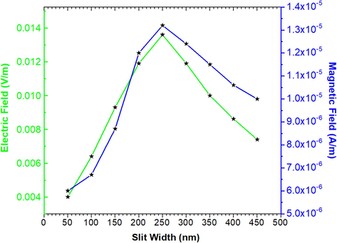
This study examines models with varying sizes of a narrow opening, ranging from 50 to 450 nm, using near-field analysis. The highest amount of light corresponds to the best value for the size of the opening.
5 Conclusion
The Cu/air 1D nanograting design device investigated with the FEA method by using the RF module of COMSOL Multiphysics. It is interesting to note that 250 nm optimum slit width is achieved with SPR of 730 nm for 1D Cu nanograting with fixed periodicity 700 nm and thickness of 50 nm. On the basis of on all above facts and figures shows that optimum slit width almost one third of the periodicity which is relevant to higher plasmonic mode, the normal electromagnetic field component well matched with the optimum width of 250 nm, the coupling efficiency of 90 % achieved by using the present 1D Cu nanograting device at optimum slit width of 250 nm and the sensitivity of 2166.06 calculated. Sensitive 2166.06 means that every time the refractive index changes by one unit (Δn), the resonant wavelength (λ) of the sensor's SPR will move 2166.06 which is higher value of sensitivity and higher sensitivity value means that the sensor can detect smaller differences in the refractive index. Such devices used as plasmonic sensor. This is good for situations where it's important to have a high sensitivity, like in biochemical sensing, environmental monitoring, or medical diagnostics.
CRediT authorship contribution statement
Zain Ashfaq: Conceptualization, Writing – review & editing. Tahir Iqbal: Supervision, Resources. Sayed M. Eldin: Writing – original draft, Visualization. Mohammad Mahtab Alam: Investigation, Methodology, Funding acquisition. Laila A. Al-Essa: Funding acquisition, Validation, Formal analysis. Tahir Iqbal: Data curation, Validation. Ahmed M. Galal: Project administration, Software.
Acknowledgment
Princess Nourah bint Abdulrahman University Researchers Supporting Project number (PNURSP2024R443), Princess Nourah bint Abdulrahman University, Riyadh, Saudi Arabia. The authors extend their appreciation to the Deanship of Research and Graduate Studies at King Khalid University for funding this work through Large Research Project under grant number RGP2/29/45.
Declaration of competing interest
The authors declare that they have no known competing financial interests or personal relationships that could have appeared to influence the work reported in this paper.
References
- Comparative dynamics of mixed convection heat transfer under thermal radiation effect with porous medium flow over dual stretched surface. Sci. Rep.. 2023;13(1):12827.
- [Google Scholar]
- Scrutinization of slip due to lateral velocity on the dynamics of engine oil conveying cupric and alumina nanoparticles subject to Coriolis force. Math. Probl. Eng.. 2022;2022:1-13.
- [Google Scholar]
- Exploration of heat and mass transfer subjected to first order chemical reaction and thermal radiation: Comparative dynamics of nano, hybrid and tri-hybrid particles over dual stretching surface. Int. Commun. Heat Mass Transfer. 2023;146:106916
- [Google Scholar]
- Review of Different CdS/TiO2 and WO3/g-C3N4 composite based photocatalyst for hydrogen production. Arab. J. Chem.. 2023;105024
- [Google Scholar]
- Enhancing on/off ratio of a dielectric-loaded plasmonic logic gate with an amplitude modulator. Sci. Rep.. 2023;13(1):5020.
- [Google Scholar]
- Enhanced extraordinary optical transmission and refractive-index sensing sensitivity in tapered plasmonic nanohole arrays. Nanotechnology. 2019;30(33):335201
- [Google Scholar]
- Numerical investigation on multiple resonant modes of double-layer plasmonic grooves for sensing application. Nanomaterials. 2020;10(2):308.
- [Google Scholar]
- Evaluation of 1-dimensional nanomaterials release during electrospinning and thermogravimetric analysis. Indoor Air. 2021;31(6):1967-1981.
- [Google Scholar]
- Surface plasmon based plasmonic sensors: A review on their past, present and future. Biosensors and Bioelectronics: X. 2022;11:100175
- [Google Scholar]
- Numerical investigation of heat and mass transfer in three-dimensional MHD nanoliquid flow with inclined magnetization. Sci. Rep.. 2024;14(1):1207.
- [Google Scholar]
- Nonlinear Hall effect as a local probe of plasmonic magnetic hot spots. Phys. Rev. B. 2021;104(7):075434
- [Google Scholar]
- Optimization of 1D Silver Grating Devices for Extraordinary Optical Transmission. Plasmonics. 2019;14(5):1099-1104.
- [Google Scholar]
- Surface-enhanced Raman scattering (SERS) on 1D nano-gratings. Plasmonics. 2020;15:1053-1059.
- [Google Scholar]
- Fast multipole boundary element method for the acoustic analysis of finite periodic structures. Computer Methods in Applied Mechanics and Engineering. 2022;391:114528
- [Google Scholar]
- Jia, H., Tsoi, C. C., Abed, A. E., Yu, W., Jian, A., Sang, S., . . . Reviews, P. (2023). Metallic Plasmonic Nanostructure Arrays for Enhanced Solar Photocatalysis. 2200700.
- Plasmonic fanoholes: on the gradual transition from suppressed to enhanced optical transmission through nanohole arrays in metal films of increasing film thickness. Optical Materials Express. 2019;9(3):1404-1415.
- [Google Scholar]
- Analysis of 1 Dimensional Photonic Crystal Optical Limiters. International Journal of Convergence in Healthcare. 2023;3(2):81-86.
- [Google Scholar]
- Encoding Mie, plasmonic, and diffractive structural colors in the same pixel. Nanophotonics. 2023;12(16):3341-3349.
- [Google Scholar]
- An efficient large-area grating coupler for surface plasmon polaritons. Plasmonics. 2012;7(2):269-277.
- [Google Scholar]
- Reusable, non-invasive, and ultrafast radio frequency biosensor based on optimized integrated passive device fabrication process for quantitative detection of glucose levels. Sensors. 2020;20(6):1565.
- [Google Scholar]
- Hybrid anisotropic plasmonic metasurfaces with multiple resonances of focused light beams. Nano Lett.. 2021;21(20):8917-8923.
- [Google Scholar]
- Orange Pectin Mediated Growth and Stability of Aqueous Gold and Silver Nanocolloids.. 2015;341:28-36.
- Computational study of Cattaneo-Christov heat flux on cylindrical surfaces using CNT hybrid nanofluids: A solar-powered ship implementation. Case Studies in Thermal Engineering. 2023;45:102959
- [Google Scholar]
- Interactive structural color displays of nano-architectonic 1-dimensional block copolymer photonic crystals. Sci. Technol. Adv. Mater.. 2023;24(1):2156256.
- [Google Scholar]
- Atomistic and coarse-grained simulations reveal increased ice nucleation activity on silver iodide surfaces in slit and wedge geometries. Atmos. Chem. Phys.. 2022;22(15):10099-10114.
- [Google Scholar]
- Numerical modeling of acousto–plasmonic coupling in metallic nanoparticles. J. Phys. Chem. C. 2020;124(22):12120-12133.
- [Google Scholar]
- Shih, Y., Krishnan, D., Durand, F., Freeman, W. T., 2015. Reflection removal using ghosting cues. Paper presented at the Proceedings of the IEEE conference on computer vision and pattern recognition.
- Shurcliff, W. A. J. S. E. (1974). Transmittance and reflection loss of multi-plate planar window of a solar-radiation collector: Formulas and tabulations of results for the case n= 1· 5. Transmission (T) and Reflection (R) through glass to air, 16(3-4), 149-154.
- Design of an unclad single-mode fiber-optic biosensor based on localized surface plasmon resonance by using COMSOL Multiphysics 5.1 finite element method. Appl. Opt.. 2022;61(21):6257-6267.
- [Google Scholar]
- Research advances on surface plasmon resonance biosensors. Nanoscale. 2022;14(3):564-591.
- [Google Scholar]
- Optical Design of Organic Solar Cell with Hybrid Plasmonic System.. 2011;19(17):15908-15918.
- Tilted circularly polarized beam microstrip antenna with miniaturized circular sector patch under wideband dual-mode resonance. IEEE Trans. Antennas Propag.. 2020;68(9):6580-6590.
- [Google Scholar]
- Localized surface plasmon resonance for enhanced electrocatalysis. Chem. Soc. Rev.. 2021;50(21):12070-12097.
- [Google Scholar]
- Zhou, X., Jin, B., Luo, J., Ning, X., Zhan, L., Xu, X., . . . Zhang, S. J. I. J. o. H. E., 2019. One-pot solvothermal synthesis of 1D plasmonic TiO2@ Ag nanorods with enhanced visible-light photocatalytic performance. 44(21), 10585-10592.