

Translate this page into:
Optical and electrical characteristics of p-type AlN co-doped ZnO thin films synthesized by RF sputtering
⁎Corresponding author. mokhamis@ksu.edu.sa (Mohammed A. Khamis)
-
Received: ,
Accepted: ,
This article was originally published by Elsevier and was migrated to Scientific Scholar after the change of Publisher.
Peer review under responsibility of King Saud University.
Abstract
Zinc oxide (ZnO) has attracted significant interest due to its exceptional material characteristics like its wide band gap (3.37 eV) and the high exciton binding energy. However, the application of ZnO is constrained by the difficulty in obtaining P-type samples. In this study, p- type ZnO thin films were fabricated using the co-doping technique with ZnO and AlN targets. Different RF powers were used for ZnO to deposite the films. However, the power on AlN target was fixed at 90 W. The structural, optical and electrical properties of the prepared films were inspected. The results of XRD showed that all the films exhibited ZnO (0 0 2) peak of wurzite structure. The UV emission peaks (3.24 eV–3.53 eV) identified in PL spectra is possibly due to the recombination of free excitons. The Raman peaks which shown at 576.22 cm−1 and 274 cm−1 denote ZnO:AlN and ZnO:N respectively. The Hall measurements of the films deposited at RF powers of 250 W and 200 W for ZnO target exhibited n-type conduction with corresponding mobilities of 2.75 cm2 V−1 s−1 and 1.58 cm2 V−1 s−1 respectively with electron concentrations of 2.35 × 1018cm−3 and 5.26 × 1018cm−3, respectively. However, the films deposited using RF powers of (150, 175) W and 225 W for ZnO target exhibited p-type conduction with hole concentrations of 2.14 × 1017 cm−3, 2.37 × 1019 cm−3 and 3.68 × 1021 cm−3 with corresponding mobilities of 9.21 cm2 V−1 s−1, 0.129 cm2 V−1 s−1 and 3.41 × 10⁻³ cm2 V−1 s−1 respectively. Therefore, RF power values of (150, 175) W and 225 W might be ideal for dopants activation to obtain p-type ZnO.
Keywords
Optical properties
Zinc oxide
X-ray diffraction
Electrical properties

1 Introduction
In recent times, Zinc oxide (ZnO) has garnered significant attention due to its exceptional material properties that include wide band gap (3.37 eV) and high exciton binding energy (60 meV), which makes it suitable for a wide array of applications like gas sensors and solar cell applications (Ozgur et al., 2005, Lau, 2005, Alivov et al., 2003). However, the complexity of obtaining P-type ZnO samples effect in the application of ZnO in optoelectronics. ZnO is characterized by n-type conductivity as a result of oxygen vacancies and zinc interstitial. For ZnO p-type, Nitrogen has been treated as an option for doping ZnO. However, ZnO has a low N solubility, which introduces a relatively deep acceptor level. To reduce the acceptor ionization energy and to improve the solubility of N in ZnO, Yamamto (Yamamoto, 2002) proposed a codoping technique to get p-ZnO.
ZnO thin films could be synthesized using a differnt techniques like (RF) sputtering (Rusu et al., 2007, Hezam, 2007, Ohgaki et al., 2003, Ryu and Zhu, 2000). The technique of RF sputtering has attracted immense interest as the properties of the ZnO films can be regulated by modifying the sputtering conditions. This is imperative since the structural, electrical and ZnO films optical properties are dependent on the conditions of preparation like substrate type, film thickness, deposition pressure, substrate temperature, RF power and annealing temperature, as reported in earlier studies (Ismail and Abdullah, 2013a, Ismail and Abdullah, 2013b, Ismail and Abdullah, 2013c, Ismail et al., 2015). Therefore, this study fabricates p- type ZnO thin films using the co-doping technique with ZnO and AlN targets. To determine the effect of modifying preparation conditions, the films were deposited at different RF powers for ZnO target. However, the power on AlN target was fixed at 90 W.
2 Experimental
AlN co-doped ZnO thin films were synthesized on type n-Si (1 0 0) and glass slide substrates through RF sputtering, by means of high purity ZnO target and high purity of AlN target. Acetone was used to wash the substrates and isopropanol in an ultrasonic bath for a duration of 15 min then subsequently rinsed with deionized water. Afterwards, Edwards A500 RF sputtering unit was used where the substrates were fixed to a rotating substrate holder, which is placed at 10 cm distance above the ZnO target. Argon (Ar) and Nitrogen (N2) of high purity (99.99%) were utilized for the sputtering of the target. Nitrogen and Argon were combined at a ratio of 80:20 to prepare the thin films. The pressure inside the chamber was maintained at 2 × 10⁻² mbar throughout the sputtering process. Then, the films were deposited at 90 W for the AlN target and at different RF powers for ZnO target for about 50 min. The conditions of the AlN co-doped ZnO films deposition were shown in Table 1.
Deposition parameters
Conditions
Operation pressure
0.02 mbar
Sputtering gases
(Ar: (N2) = (20:80)
Power on targets
ZnO target ≡ (250, 225, 200, 175 and150)W with AlN target ≡ 90 W
Samples (ANZO41, ANZO40, ANZO39, ANZO38 and ANZO37) correspondingly
Deposition temperature
Room temperature
The films optical properties were examined using Raman spectroscopy, UV–visible spectrophotometry, and Photoluminescence (PL) and. The prepared films thickness (t) was determine using F20 filmetrics. The structural thin films properties were characterized using X-ray diffractometer (source Cu Kα with λ = 1.5406 Å), while the fabricated ZnO thin films surface morphologies were studied using field emission scanning electron microscopy (FESEM). The samples electrical properties were investigated using the Hall Effect equipment (HL5500PC model).
3 Results and discussion
The prepared thin films thickness (t) was observed to be increase with the applied RF powers on ZnO target as shown in Fig. 1. This indicates that the amount of sputtered atoms from the target is proportional to the applied RF power.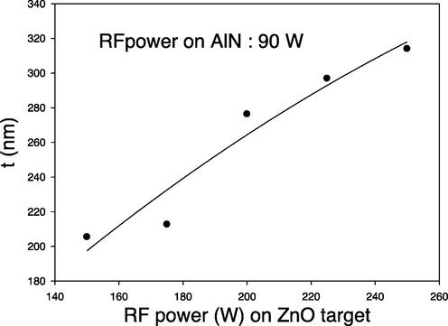
Thickness of AlN: ZnO thin films as a function of RF power on Si substrates.
The XRD spectra for the synthesized AlN doped ZnO films is shown in Fig. 2. The current research is comparing the XRD spectra for AlN doped ZnO with the undoped ZnO in a previous work (Ismail and Abdullah, 2013a, Ismail and Abdullah, 2013b, Ismail and Abdullah, 2013c). It was found that the (0 0 2) ZnO phase is discernible in all the films and the average value of 2θ and d of the undoped ZnO is equal to 34.1841° and 2.6229 Å respectively (Ismail and Abdullah, 2013a, Ismail and Abdullah, 2013b, Ismail and Abdullah, 2013c). The AZO 40 sample displayed the lowest d-spacing value of 0.26174 nm comparing with the undoped ZnO, which can be attributed to the Al ions substitution with Zn ions where the radius of Al+3 ion (0.53 Å) is smaller than the radius of Zn+2 ion (0.74 Å). Therefore, the (0 0 2) peak position of the AZO 40 sample shifted to a higher diffraction angle. Secondly, the sample showed the smallest calculated value of the FWHM of ZnO (0 0 2) peak comparing with the other samples. So, the abnormal behavior in the crystallite size was shown for AZO40 sample. However, the d-spacing value of AZO 37, AZO 38, AZO 39 and AZO 41 samples is larger than the d-spacing value of the undoped ZnO, probably due to the substitution of N−3 ions on O−2 ions site, where the radius of N−3 ion (1.46 Å) is larger than the radius of O−2 ion (1.40 Å). Therefore, the (0 0 2) peak position shift to a smaller angle. FWHM of ZnO (0 0 2) peak was used to calculate the crystallite size (D) in the synthesized thin films using the following Scherrer’s formula.
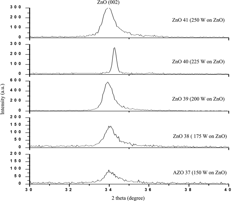
XRD spectra of AlN: ZnO thin films at a different of RF power on Si substrates.
where θ is the Bragg angle, λ denotes the incident X-ray wavelength and β represents the full width at half maximum (FWHM). Table 2 summarizes the values found from XRD technique for (0 0 2) AlN: ZnO thin films phase.
Sample
2 ɵ (°)
FWHM(˚)
d (Å)
c (Å)
D(nm)
AZO 37
33.9659
0.3936
2.6394
5.2788
22.05
AZO 38
34.0759
0.3936
2.6311
5.2622
22.06
AZO 39
33.8877
0.3936
2.6453
5.2906
22.05
AZO 40
34.2604
0.1968
2.6174
5.2348
44.14
AZO 41
34.0228
0.3936
2.6351
5.2702
22.06
The AlN: ZnO films EDX analysis are presented in Table 3, where minor concentrations of nitrogen (0.09–3.96 at %) was identified. It also important to notice that N and Al were incorporated at different concentration into the prepared AlN: ZnO thin films although the RF sputtering power on AlN was fixed at 90 W. This could be explained as following, introduction of nitrogen during the fabrication process (80%N2:20%Ar) and using different powers in ZnO target could have eventually led to the formation of (N2)O donors or (N)O acceptors in the films resulting in different concentration of N in the prepared thin films. The other possible mechanism is due to the formation of N-Al-N complex, arising from AlZn (Al on Zn) and NO (N on O) according to the suggestions of Yamamoto’s model. This configuration (N-Al-N) can stabilize ionic charges, enhances strong attractions between donor (Al) and acceptor (N) and reduces the repulsive interactions between the acceptors. In addition, the binding energy of the donor can be raised and the binding energy of the acceptor can be reduced, resulting in shallower acceptor that could improve the solubility of N-Al-N complex in the prepared of ZnO films (Yamamoto, 2002). The films surface morphology was measured using FESEM (Fig. 3). As observed in the FESEM images, the particles of the thin films grew larger as the RF power applied on ZnO target increased.
Sample
NK (at %)
O K (at %)
Al K (at %)
Zn L (at %)
AZO 37
3.59
55.17
3.66
37.59
AZO 38
0.09
56.27
4.92
38.73
AZO 39
3.10
54.43
2.81
39.66
AZO 40
3.96
53.72
2.91
39.41
AZO 41
2.76
51.18
2.07
43.99
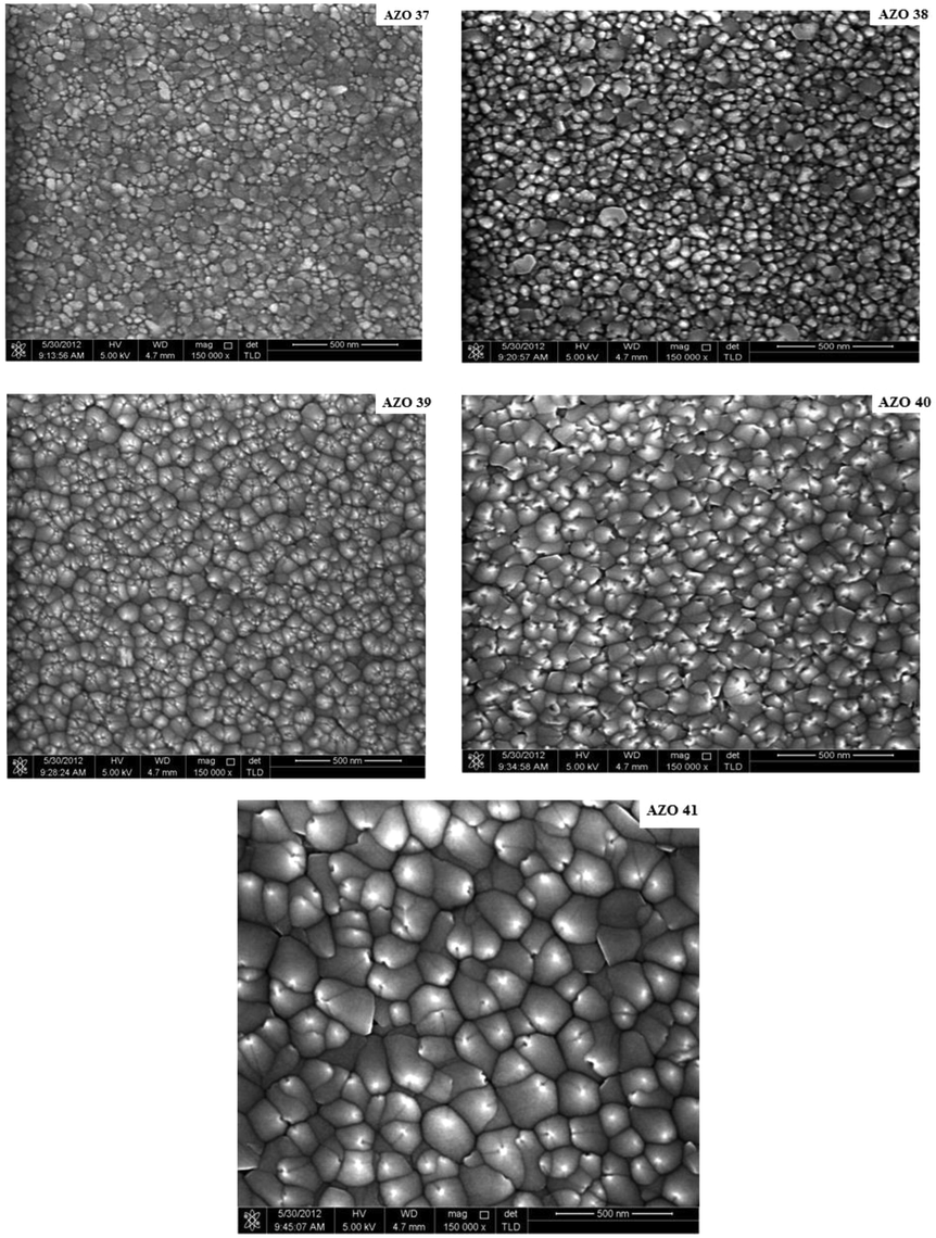
FE-SEM images of AlN: ZnO thin films at different RF powers on Si substrates.
Ultraviolet and visible (UV–vis) transmission spectrometer (model: U-2000 HITACHI) was used to determine the energy band gap (Eg). The light produced by light grating is splitted in to two equal intensity beams (reference beam and sample beam) using a half mirror. Then, the two beams passed through the reference and the sample cuvettes and their intensities are then measured by the detectors. The intensity of the reference beam is defined as I0 and the intensity of the sample beam is defined as I. The ratio (I/I0) is defined as the transmittance (Ti). The relation between the absorption coefficients α determined from the transmittance spectra and the photon energy (E) is given by; where Eg is the energy band gap of the semiconductor, t is the thickness of the films and A is a constant. Therefore, a plot of (αE)2 versus photon energy E produced a straight line that cut the photon energy axis at the energy band gap value. The photon energy can be calculated using the following equation: where h is the planck’s constant, c is the speed of light in vacuum and (λ) is the wavelength.
Fig. 4 revealed a good optical transmittance of ZnO doped with AlN thin films that exceeds 70% in the visible range. Also, it is important to notice from the XRD analysis that, only AZO 40 sample displayed d-spacing value of 0.26174 nm which was smaller than the d-spacing of the undoped ZnO (0.26229 nm) (Ismail and Abdullah, 2013a, Ismail and Abdullah, 2013b, Ismail and Abdullah, 2013c). Secondly, AZO 40 showed the largest value of the crystallite size of (44.14 nm) comparing with the other samples (AZO37, AZO38, AZO39 and AZO41). So, a different behavior in UV–vis spectra for this samples was shown which could be attributed to the substitution of Zn ions with Al ions.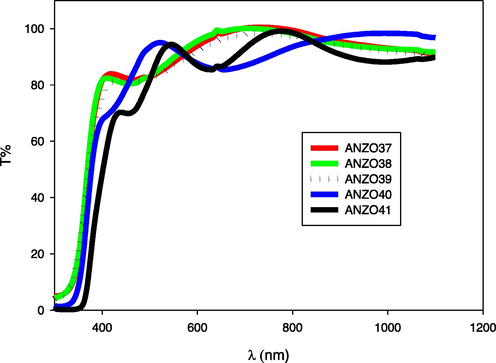
AlN: ZnO Transmittance spectra of the prepared thin films on glass substrates at different RF powers.
Fig. 5 displays the graph of (αE)2 versus E for the prepared samples that produces a direct energy band gap values of 3.31 eV, 3.40 eV, 3.39 eV, 3.41 eV and 3.40 eV for the prepared films with RF power (ZnO target) of 250, 225, 200, 175 and 150 W, respectively. As shown in Fig. 6, the optical direct energy band gap shifted from 3.41 eV to 3.31 eV with decreasing Al concentration, which is consistent with earlier related reports (Zi-qiang et al., 2006, Burstein, 1954, Moss, 1954), and is referred to as the Burstein- Moss effect.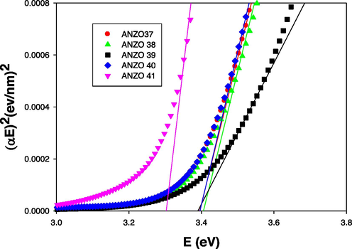
(αE)2 versus E of AlN: ZnO films on glass at various RF powers on glass substrates.
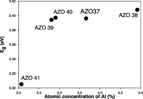
Direct energy gap (Eg) versus Al at % concentration of AlN: ZnO thin films at different RF powers on glass substrates.
The photoluminescence (PL) characteristics of the prepared AlN:ZnO thin films were obtained at room temperature in the photon energy range of 1.24 eV–4.1 eV. All the films showed UV emission peaks (Fig. 7) attributed to the free exciton recombination indicating a good crystalline structure and also good optical properties (Ismail and Abdullah, 2013a, Ismail and Abdullah, 2013b, Ismail and Abdullah, 2013c, Kumar et al., 2009). Due to the Moss-Burstein effect the UV emission bands shifted to higher energy (from 3.26 eV to 3.53 eV) with increase in Al concentration from 2.07% to 3.66% which is in conformity with the optical transmittance results. It is important to see that the green emission (2.1 eV–2.3 eV) in the present films show low intensity of (100–180 a.u.) in comparing with our published undoped ZnO (450–1000 a.u.) (Ismail and Abdullah, 2013a, Ismail and Abdullah, 2013b, Ismail and Abdullah, 2013c). The lowing of the intensity indicate the successes doping of AlN: ZnO and also reducing the effect of the intrinsic defects in this films (Kumar et al., 2014, Verma et al., 2015). As a result, the dopant-induced in ZnO films will be effect in the electrical properties as will be shown latter.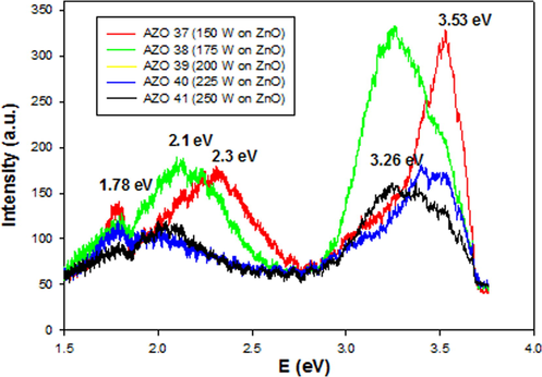
The PL spectra of AlN: ZnO thin films at different RF powers on Si substrates.
The AlN doped ZnO thin films Raman spectra is shown in Fig. 8 (a). It is important to detect in the present work a new peak at 274 cm−1 for all the prepared thin film samples which was not shown in the undoped ZnO. This peak denoted to the presence of nitrogen in all the prepared samples (Zhao et al., 2010). Whereas there is a shift in the peak which was observed at 576.22 cm−1 in the present research comparing with the previous work for undoped ZnO (573.72 cm−1) (Ismail and Abdullah, 2013a, Ismail and Abdullah, 2013b, Ismail and Abdullah, 2013c). This shift indicate the successes doping of AlN :ZnO films which is attributable to A1 (LO) modes in agreement with other published work (Zhao et al., 2010, Cerqueira et al., 2010). These modes intensity (274 cm−1 and 576.22 cm−1) are linearly related to the concentration of the nitrogen, which is a valuable tool for evaluating the relative nitrogen concentration in the films (Kaschner et al., 2002). Thus, it can be inferred that incorporation of nitrogen into the ZnO films is influenced by the magnitude of RF power applied on ZnO target. However, it is imperative to note that there is a disparity between the results of Kascher (Kaschner et al., 2002) and the EDX (Table 3) presented in this study, since the EDX presented results only at one point on the samples and offered primary information on the nitrogen in the samples. Nonetheless, this research seems to be more consistent with that of Kascher (Kaschner et al., 2002) who introduced more accurate results which could be used to find the relative concentration of nitrogen in the films.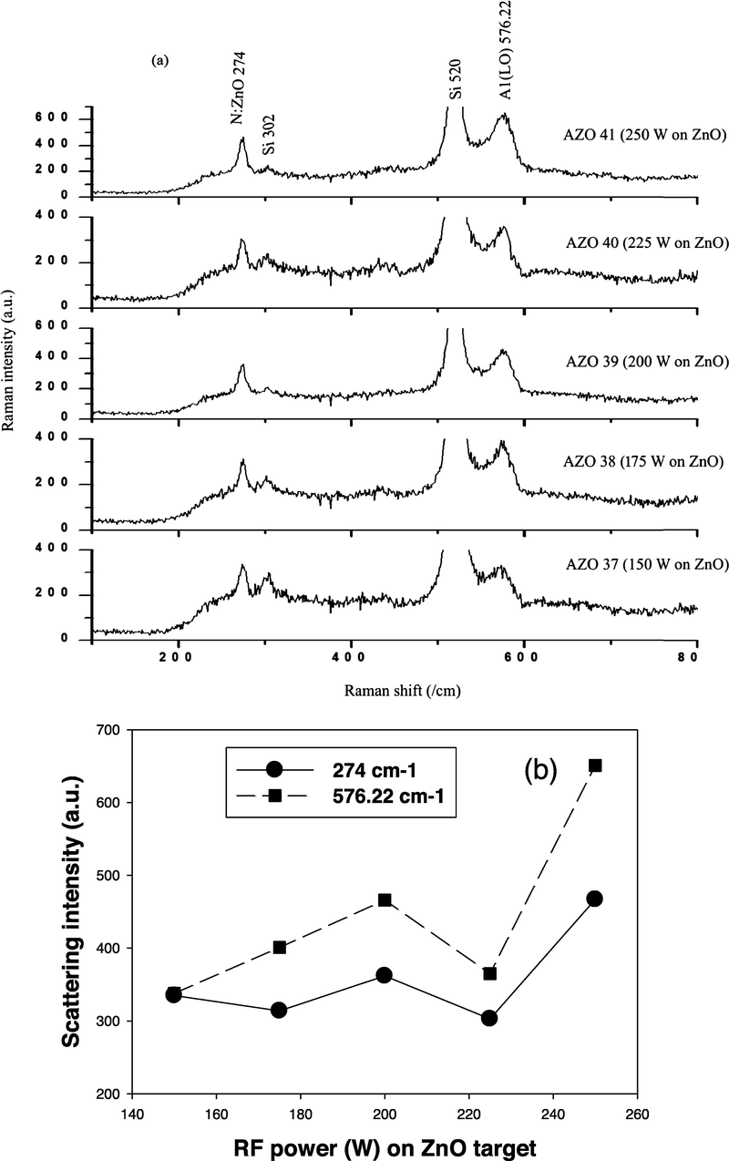
(a) Raman spectra of AlN: ZnO thin films and (b) modes intensity variation at different RF on Si substrates.
The electrical properties of the synthesized AlN doped ZnO thin films (n-type and p-type conductivities) are presented in Table 4. The concentration, resistivity and mobility of the carrier were measured as a function of RF powers on ZnO target. AZO 37, AZO 38 and AZO 40 samples displayed p-type conductivity with hole concentrations of 2.14 × 10+17 cm−3, 2.37 × 10+19 cm−3 and 3.68 × 10+21 cm−3 respectively. The p-type conductivity in the AZO 40 sample can be attributed to the substitution of Zn+2 ions site (0.074 nm) with Al+3 ions (0.053 nm) and the development N-Al-N complex which serves as a shallow acceptor. This is corroborated by the presence or incidence of nitrogen in the sample as deduced from the XRD, Raman and EDX results as well as the lesser d-spacing value (0.26174 nm) compared to that of undoped ZnO (0.26229 nm). On the other hand, the p-type conductivity in AZO 37 and AZO 38 samples can be attributed to the substitution of O−2 ions site (0.140 nm) with N−3 ions (0.146 nm) and the development of (N2)O donors and (N)O acceptors. Nevertheless, (N)O acceptors effect more than of (N2)O donors effect , leading to the creation of p-type conductivity in these samples. This is confirmed by the presence of nitrogen detected by Raman, XRD, EDX results, and the larger d-spacing values of the samples (0.26394 nm and 0.26311 nm, respectively) as compared to that of the pristine/undoped ZnO (0.26229 nm).
Sample
Thickness, t (nm)
Resistivity (Ωcm)
Mobility (cm2 V−1s−1)
Carrier concentration (cm−3)
AZO37
210
3.170
9.21
+2.14 × 10+17
AZO38
220
2.040
0.129
+2.37 × 10+19
AZO39
276
0.751
1.58
−5.26 × 10+18
AZO40
280
0.498
3.41 × 10⁻³
+3.68 × 10+21
AZO41
314
0.966
2.75
−2.35 × 10+18
Conversely, the AZO 39 and AZO 41 samples displayed n-type conductivity with electron concentrations of 5.26 × 10+18 cm−3 and 2.35 × 10+18 cm−3, respectively. Raman, XRD and EDX results confirmed the presence of nitrogen in these samples. In addition, the larger d-spacing values of the samples (0.26453 nm and 0.26351 nm, respectively) as compared to that of undoped ZnO (0.26229 nm) implies N−3 ions substituted O−2 ions. Nonetheless, the effect of (N2)O donors and the other intrinsic donors exceeds that of (N)O acceptors, leading to the formation of n-type conductivity in these samples. From Raman spectra, the dependence of mode intensity on the RF power applied to ZnO is presented in Fig. 8 (b). It can be deduced that nitrogen absorption into the samples increases with higher RF power of ZnO, possibly due to higher intensity of 274 cm−1 and 576.22 cm−1 modes for ZnO:N and ZnO:AlN, respectively. Therefore, RF power values of (150, 175 and 225) W may be ideal conditions to obtain p-type ZnO.
4 Conclusion
The p-type ZnO was obtained via the co-doping of AlN and ZnO. The deposition of the films for ZnO target was occurred at different RF powers of (150, 175, 200, 225 and 250) W and 100 W for AlN target. All the films exhibited ZnO (0 0 2) peak of wurzite structure. The observed Raman peaks of 274 cm−1 and 576.22 cm−1 are associated with the incorporation of N and AlN in the ZnO films. From Hall measurements, the deposited thin films at RF powers of (150, 175 and 225) W for ZnO target and 90 W for AlN target exhibit conduction of p-type with hole concentrations of 2.14 × 10+17cm−3, 2.37 × 10+19 and 3.68 × 10+21cm−3 with corresponding mobilities of 9.21 cm2 V−1 s−1, 0.129 cm2 V−1 s−1 and 3.41 × 10⁻³ cm2 V−1 s−1, respectively. The p-type conductivity in the AZO40 (225 W) sample can be attributed to the substitution of Zn+2 ions site (0.074 nm) with Al+3 ions (0.053 nm) as confirmed using XRD and the development N-Al-N complex which serves as a shallow acceptor. For AZO37(150 W) and AZO38 (175 W) samples, the p-type conductivity can be attributed to the substitution of O−2 ions site (0.140 nm) with N−3 ions (0.146 nm) and the development of (N2)O donors and (N)O acceptors. Nevertheless, (N)O acceptors effect more than of (N2)O donors effect, leading to the creation of p-type conductivity in this samples.
Acknowledgements
The authors extend their appreciation to the Deputyship for research & innovation, “Ministry of Education” in Saudi Arabia for funding this research work through the project number IFKSURG-1440-037.
Declaration of Competing Interest
The authors declare that they have no known competing financial interests or personal relationships that could have appeared to influence the work reported in this paper.
References
- The changes in structural and optical properties of (ZnO:AlN) thin films fabricated at different RF powers of ZnO target. Ceram. Int.. 2013;39:S441-S445.
- [Google Scholar]
- The structural and optical properties of ZnO thin films prepared at different RF sputtering power. J. King Saud Univ. – Sci.. 2013;25(3):209-215.
- [Google Scholar]
- The effect of substrate temperatures on the structural and optical properties of cosputtered ZnO and AlN thin films. Adv. Mater. Res.. 2013;626:25-28.
- [Google Scholar]
- The effect of substrate temperatures on the structural, optical and electrical properties of N-Al codoped ZnO thin films. J. Luminescence. 2015;164:69-75.
- [Google Scholar]
- Nitrogen-related local vibrational modes in ZnO:N. Appl. Phys. Lett.. 2002;80:1909.
- [Google Scholar]
- Fabrication and characterization of n-ZnO/p-AlGaN heterojunction light-emitting diodes on 6H-SiC substrates. Appl. Phys. Lett.. 2003;83(23):4719-4721.
- [Google Scholar]
- Red shift of the band-edge photoluminescence emission and effects of annealing and capping agent on structural and optical properties of ZnO nanoparticles. J. Alloys Comp.. 2015;625:122-130.
- [Google Scholar]
- Hezam, M.S., 2007. Synthesis and Characterization of ZnO Thin Films. 2007. Physics. Dhahran, Saudi Arabia, KFUPM. Master of Science.
- Laser action in ZnO nanoneedles selectively grown on silicon and plastic substrates. Appl. Phys. Lett.. 2005;87(1)
- [Google Scholar]
- M.F. Cerqueira, A.G. Rolo, T. Viseu, J. Ayres de Campos, T. de Lacerda-Arôso, F. Oliveira, M.I. Vasilevskiy, E. Alves, 2010. Raman study of doped-ZnO thin films grown by rf sputtering. Phys. Status Solidi (c), (7) 2290-2293.
- M. Kumar, S.-K. Kim, S.-Y. Choi, 2009. Formation of Al-N co-doped p-ZnO/n-Si (100) heterojunction structure by RF co-sputtering technique. Appl. Surface Sci. (256) 1329-1332.
- Growth condition dependence of morphology and electric properties of ZnO films on sapphire substrates prepared by molecular beam epitaxy. J. Appl. Phys.. 2003;93(4):1961.
- [Google Scholar]
- A comprehensive review of ZnO materials and devices. J. Appl. Phys.. 2005;98(4):041301-42103.
- [Google Scholar]
- Preparation and characterization of ZnO thin films prepared by thermal oxidation of evaporated Zn thin films. Superlatt. Microstruct.. 2007;42(1–6):116-122.
- [Google Scholar]
- Optical and structural properties of ZnO films deposited on GaAs by pulsed laser deposition. J. Appl. Phys.. 2000;88(1):201.
- [Google Scholar]
- The interpretation of the properties of indium antimonid. Proc. Phys. Soc. London Ser. B. 1954;67:775.
- [Google Scholar]
- Effect of Eu doping on the photoluminescence properties of ZnO nanophosphors for red emission applications. Appl. Surface Sci.. 2014;308:419-430.
- [Google Scholar]
- Al-doping effects on structure, electrical and optical properties of c-axis-orientated ZnO: Al thin films. Mater. Sci. Semicond. Process.. 2006;9:132-135.
- [Google Scholar]
- A new phase and optical properties of the N-doped ZnO film. Mater. Res. Bullet.. 2010;45:1046-1050.
- [Google Scholar]