

Translate this page into:
Modeling and analysis of debonding in a smart beam in sensing mode, using variational formulation
⁎Corresponding author. mursaleen@nitsri.net (Mohammad Mursaleen Butt),
-
Received: ,
Accepted: ,
This article was originally published by Elsevier and was migrated to Scientific Scholar after the change of Publisher.
Peer review under responsibility of King Saud University.
Abstract
Using basic electro-elastic formulation and variational formulation, a higher order finite element model has been developed for the analysis of debonding in a smart cantilever beam. Full length piezo patch embedded at the top and bottom of the aluminium core has been assumed to be de-bonded. The debonding has been incorporated at the interfaces between piezo patches and the core, at the mid span of the beam for one third length of the beam. The effect of debonding in sensing mode has been analysed by presenting the induced potential, axial displacement, axial/transverse electric field and stresses for fully bonded and de-bonded smart cantilever beam. The variation in electric potential, electric field, axial displacement/strain/stress and shear strain/stress observed in case of debonding demonstrates that the mechanics of debonding is complex coupled electro-mechanical behaviour. In the de-bonded beam, the induced potential at the free piezo surface and at the interfaces shows a sinusoidal variation from root to the tip as compared to the linear variation in bonded beam. This is attributed to the non-linear bending moment variation from root to the tip in case of de-bonded beam. The maximum stress in debonding increases nearly 1.5 times to that of bonded beam sensing at various locations.
Keywords
Smart beam
PZT-5H
Actuation
Sensing
Bonding
De-bonding

Nomenclature
-
material elastic constants
-
electric field
-
dielectric constants
-
stiffness matrix
-
polarisation
- Q
-
electric charge per unit area
-
heat flux
- ds
-
elemental surface area
- dv
-
elemental Volume
- z
-
thickness coordinate direction
-
with respect to i, where
-
permittivity of free space
-
strain tensor
-
stress tensor
-
piezo electric constants
-
axial and transverse displacement
-
surface Traction
-
temperature difference
-
poisson ratio
-
variation
Nomenclature
1 Introduction
Piezo-electric sensors and actuators have been analysed, tested and used in the design and development of smart structures. This has applications for all the air borne and ground borne structures. The control systems employed in smart structures have been widely used for health monitoring of structures. To make a structure smart, piezo patches have been embedded on the structural surfaces. A piezo patch under the application of electric voltage may contract or strain and hence can be used as an actuator. Strain can be sensed from the host structure by induction of electric potential in the embedded piezo patch. Moreover one can assume an adhesive layer between piezo patch and metallic host material or brazing (no adhesive layer between piezo and host material). In the current study piezo patch has been assumed to be brazed on the metallic host material. Based on this proposition, analysis of partial or full de-bonding between piezo and metallic host material has been carried out. De-bonding can take place in the vibrations of smart structures attached to helicopters, missile guidance and control systems, satellites, naval and military artillery, automobiles, civil structures and many other smart structures.
Due to fatigue, thermal stresses and non-uniform interface stresses in smart structures, de-bondings occur which affect the structural effectiveness. If these de-bondings can be sensed at the right time, structural failure can be eliminated. In the current research, electro-thermo-elastic formulation has been developed for analysing de-bondings in smart structures. Electro-thermo-elasticity has been reviewed with regards to various electro-thermo-elastic coupling effects. Electro-thermo-elastic equations have been modified using some useful assumptions to present the equations in useful form. Procedures have been evolved for solving electro-thermo-elastic equations. Variational formulation has been developed from electro-thermo-elastic formulation. Layer-by-layer finite-element-modeling has been carried out based on electro-thermo-elastic variational formulation. In this paper analysis for electric field, strain and stress in transverse and axial direction has been carried out in sensing with and without debonding. All this is useful feed back for a designer to design a smart structural control or health monitoring kit.
Piezoelectric materials are known to transform electric loads into mechanical effects and vice versa, this phenomenon has made them most suitable for the application as sensors and actuators (Cady, 1964; Ikeda, 1990). Focusing their use in the field of structural engineering with the aim to make the structures smart, piezo layers have been either sandwiched between the metallic layers (shear mode phenomena) or bonded on the top and bottom of metallic layer (extensional mode phenomena). The piezo layers act both as mechanical strain sensors as well as electrically actuated actuators. The laminated structure so designed needs to be analysed for sensing, actuation and shape control. This needs an electro-thermo-elastic formulation of an electrically polarised medium. A fundamental smart structure starts with the design of a metallic cantilever beam bonded with piezo layers at the top and bottom. This materially heterogeneous structure is complicated for theoretical analysis. Hence a numerical technique like finite elements is required for analysis. Finite element analysis needs modeling based on electro-thermo-elastic formulation. The important research areas are actuation, sensing, shape control, structural health monitoring, de-lamination and de-bonding. The current area of research will be the study of partial or full de-bonding of a piezo layer from the host material of a metallic smart cantilever beam. Here an essential difference between de-lamination and de-bonding needs to be brought out. De-lamination refers to partial or full separation of lamina from each other in composite structures whereas de-bonding refers to partial or full separation of piezo layer from smart metallic host structure. During operation or aging a smart structure may undergo de-bonding at interfaces between piezo layer and metallic host material. This phenomenon affects the effectiveness of the structure. To sense this, a provision is to be provided in the stiffness matrix for additional degrees of freedom for de-bonded region. The generation of additional nodes due to de-bonding for a particular portion of length and their solution for displacement, strain and stress will give a sense of de-bonding in that portion.
The first static electroelastic formulation was given by R. A. Toupin in 1956 and later by Eringen and Suhubi (1964). In this formulation the authors derived the governing equations based on variational principles. Later, Tiersten (1971) derived the nonlinear governing equations of electro-thermo-elasticity by applying basic conservation laws of continuum physics to a macroscopic model. A comprehensive survey on smart technology can be found in Crawley (1994). Zhang and Sun (1996) have presented a theoretical formulation of an adaptive beam actuation problem in both extension mode (piezo patches on top and bottom of aluminum core) and shear mode (piezo patch sandwiched between aluminum layers). It has been found that shear mode actuation is advantageous over extensional mode actuation. Chattopadhyay et al. (1998) have presented a finite element formulation for coupled electro-thermo-elastic problem for smart composite plates under thermal loading using higher order displacement. They have studied the temperature variation in the composite stack for several lay-up sequences. It is shown that piezo actuation over predicts the plate deformation in the uncoupled case relative to the coupled case. Aldraihem and Ahmed (2000) have shown that the deflections obtained in first order beam theory and higher order beam theory are different for shear mode actuation.
In most of the studies (Aldraihem and Ahmed, 2000; Librescu et al., 1997; Crawley and Luis, 1987; Shen et al., 1994; Benjeddou et al., 1999; Robbins and Reddy, 1991; Ha et al., 1992), electric field E = voltage/thickness of piezopatch. This decouples the electric and mechanical phenomenon. Therefore electric potential is taken to be the quadratic variation of thickness and function of bending curvature (Ahmad et al., 2004).
Ratcliffe and Bagaria (1998) have successfully located the de-lamination in a composite beam using the gapped smoothing damage detection method. Xiaoxia et al. (2001) have established a two-dimensional de-lamination model to investigate the effect of the applied electric field on the energy release rate of the de-lamination of piezoelectric/elastic laminates. Zheng et al. (2004) have developed a solid finite element for the vibration analysis of curved smart beam. The effect on the frequencies due to de-bonding has been reported. A new interface element technology has been presented by Pantano and Avirill (2004) for predicting crack growth in laminated structures. Ahmad et al. (2004) have used higher order beam theory to bring about difference between sensing and actuation by showing the induced potentials in piezo patch at the top and bottom of the smart cantilever. The non-linearity induced because of the interaction between polarisation and electric field has been brought about by presenting the tip deflection for various actuation voltages for linear and non-linear cases. Ahmad et al. (2005) have carried out finite element layer-by-layer modeling of the smart cantilever and have presented through thickness the transverse and axial displacement, electric field, normal stress/strain and shear stress/strain. This has brought about the difference in the behaviour of smart beam in actuation and sensing. Li and Sridharan (2005) have used a cohesive layer model having strengths and initial stiffness that are characteristic of the medium in which the de-lamination crack runs; further a stress–strain relationship rather a traction-relative displacement relationship has been postulated for the material. Tan and Tong (2006) have developed a dynamic analytical model for identifying multiple de-laminations embedded in a laminated beam, which is surface bonded with an integrated magneto-strictive layer. Ahmad et al. (2006) have developed electro-thermo-elastic formulation based on conservation of momentum, angular momentum, charge, mass and energy. The complicated equilibrium and constitute equations so developed have been modified by using assumptions with regards to interaction between electric field and polarisation. The simple equations so developed have been used to develop variational and then finite element formulation. The smart cantilever problem has been analysed for validation of the results. Sateesh et al. (2008) have presented a thermodynamic hysteresis model for the analysis of smart beam. A 2-node FE is formulated by Chrysochoidis and Saravanos (2009) with nodal degrees of freedom entailing in plane and transverse displacement, electric potentials, and de-lamination relative displacements. Transient response is predicted through time integration and its pseudo Wigner-Ville distributions (PWVD) are presented for healthy and de-laminated composite beams. Analytical time frequency distributions are further correlated with similar experimental results. Ramdas et al. (2009) have made numerical and experimental investigation for the generation of a new primary Lamb mode when the incident primary anti-symmetric Lamb mode interacts with a high aspect ratio symmetric de-lamination. Su et al. (2009) have developed a Lamb-wave based damage imaging approach with the capacity to visually pin point structural damage, if any, in terms of the probability of damage occurrence at all spatial positions of the structure under interrogation. Ahmad et al. (2009) have implemented the electro-thermo-elastic formulation to model a smart fin in a micro heat exchanger. The space between fins has been controlled by piezo actuation to control the flow of fluid through exchanger. Jin et al. (2010) presented closed-form and novel formulas for calculating interface stresses and mode I and II energy release rates for an interfacial straight crack in PZT composite beams. In FEM analysis, interface element is used to model the de-bonding of adhesive interface with exponential cohesive zone model.
However in none of the above contributions, static studies on axial deformation, electric field, stress and strain due to de-bonding in smart structures has been carried out. In the present study, coupled bending-piezoelectric phenomena has been incorporated in the electric potential variation with respect to ‘z’ (thickness direction). With this proposition electro-thermo-elastic formulation has been developed and based on this, layer-by-layer finite element modeling has been carried out. The de-bonding phenomena has been incorporated by allowing additional degrees of freedom in the de-bonded portion of span in the smart cantilever. The effect of de-bonding in sensing phenomenon has been investigated.
2 Mathematical formulation
Authors from Cady (1964) to Tiersten (1971) have addressed the electro-thermo-elastic formulation using basic laws of physics. The governing equilibrium and constitute equations have been developed using conservation of momentum, angular momentum, charge, mass and energy. Using the procedures presented in Tiersten (1971), electro-thermo-elastic formulation has been developed for use in modeling the de-bonding. Formulation involves the development of three sets of equations. They are: equilibrium equations, constitutive relations and boundary conditions. The governing equations so developed have been modified by using certain assumptions. The complex equations become simple by assuming the polarisation vector parallel to the electric field vector. This makes the stress tensor symmetric and the stress strain relation linear. The unknowns are thirty-three which include three displacements, six strains, nine stresses, three electric displacements, three electric fields, three polarisation components, one electric potential, one temperature, three thermal fluxes and entropy at a point. These can be found from thirty-three governing equations. The elaborated formulation and basic finite element modeling can be found in Ahmad et al. (2004).
The static force, electrostatic and thermal equilibrium equations have been multiplied by the corresponding variations and integrated over the domain to give variational formulation as;
Stress has symmetric and non-symmetric part. If the electric field vector and the polarisation vectors are parallel then non-symmetric part of stress is zero. Using Gauss Divergence theorem to convert volume integrals into surface integrals, one can write;
The first term in the above equation leads to stiffness matrix. The second term gives electro-elastic coupling matrix. The right side of the equation gives the load vector.
2.1 The elemental stiffness matrix
For finite element modeling
functions have been used to discretise the axial displacement
, transverse displacement
and electric potential
. The stiffness matrix developed for piezo layer has an order of 32x32. The pure elastic stiffness matrix has an order of 20x20 and an electro elastic stiffness matrix has an order of 20x12. The pure electric stiffness matrix has an order of 12x12 as;
The non-piezo layer is non-polarised medium and has an order of 20x20. The degrees of freedom in the stiffnes matrix have been given as;
The global stiffness matrix
, global degrees of freedom matrix
and load vector
are related as;
3 Results and discussion
A higher order beam bending element with layer-by-layer finite element model has been used to analyse a fully piezo-patched smart aluminum-core cantilever. Tip deflection of in 10Volt actuation has been validated with known results. Multipatched beam has been validated for induced voltages in patches with Shen et al. (1994). These all validations can be seen in Ahmad et al. (2004).
Debonding has been incorporated for one-third of the middle of the span at the interfaces between piezo and the host material at the top and bottom of the cantilever. The problem has been then analysed for sensing of a tip deflection produced for 10Volt actuation in fully bonded and de-bonded case. The comparison has been brought about for induced voltage, axial deflection, axial/transverse stress/strain and electric field.
3.1 Electro-elastic analysis (Sensing)
In order to bring about the characterisation of debonding, a smart cantilever beam Fig. 1 has been chosen. The beam comprises of aluminum core embedded with full PZT-5H piezo patch at the top and bottom surfaces. The piezo patches have the polarisation axis in the positive z-direction. When this beam is actuated by 10Volt at the top and bottom surface while keeping interfaces grounded, a tip deflection of
in the negative z-direction is produced which has been already validated. Now in the beam Fig. 1 at the middle of the span, one third of the interfaces between piezo and aluminum core has been considered de-bonded. The de-bonded beam has been given a tip deflection equal to
and has been analysed for induced potential at the free surface of the piezo patches, axial deformation, axial/transverse electric field, axial/transverse strain and stress at different location series, different from the bonded results referred in Ahmad et al. (2005). The results have been presented with different ranges. The analysed de-bonded beam has the following dimensions: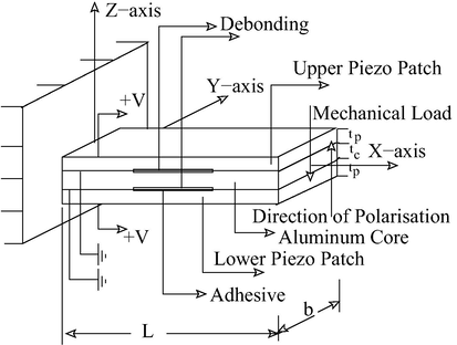
Smart Beam in Extensional Mode with Debonding.
Length, L = 100 mm
Thickness of Aluminum core,
Thickness of each piezo layer,
Total thickness of beam,
Width of beam, = unity.
The material properties of piezo patch are given in Table 1. The constitute equation for PZT-5H for electro-elastic behaviour has been given as;
PZT-5H
GPa
1.5045
1.30095
126
79.5
84.1
117
23
−6.5
23.3
17.0
Constants and refer to dielectric permittivity tensor at constant strain, components of piezoelectric constants and elastic constants respectively. The material properties of aluminium core have been taken as; modulus of elasticity = 70.3 GPa and Poisson ratio = 0.345.
3.1.1 Induced potential
Consider the example of sensing, a tip deflection of
has been considered in the problem of Fig. 1 with above dimensions. Fig. 2 shows the variation of induced potential at the top free surface of the piezo layer while keeping the interfaces between the piezo and aluminum core grounded. The induced potential for the case of fully bonded and one-third of mid span interfaces de-bonded has been presented. For fully bonded interfaces, the induced potential varies from 1.94Volt at the root to 0.0Volt at the tip for the free surfaces whereas induced potential varies from 0.935Volt at the root to 0.0Volt at the tip for the mid layer of the piezo patches in a linear fashion.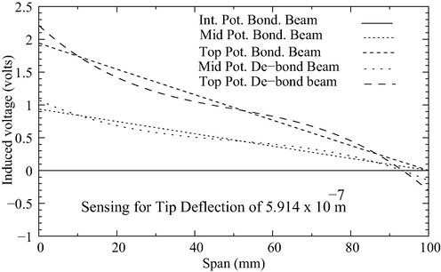
Comparison of Induced Voltage in Bonded and Debonded Beam of 16 mm Core and 1 mm Patch Smart Beam in Sensing.
For de-bonded interfaces, the induced potential varies from 2.21Volt at the root to −0.305Volt at the tip for the free surfaces whereas induced potential varies from 1.07Volt at the root to −0.152Volt at the tip for the mid layer of the piezo patches in a sinusoidal fashion. It is clear from the graph that the contractions and expansions in the piezo patches due to debonding at the middle of the span, are not smooth. The finite element model behaves properly and exhibits similar induced potential in the top and bottom piezo layers in a symmetric manner.
3.1.2 Axial displacement
Continuing with the same example as presented in Section 3.3.1. The variation of axial displacement has been given in Fig. 3. In case of fully bonded beam, it can be seen that axial displacement is zero at the root at every nodal point which is in accordance with the boundary condition that
whereas axial displacement at the tip over the surface is
. The variation of axial displacement can be seen varying linearly from bottom surface to top surface along z direction and is presented at locations
and
.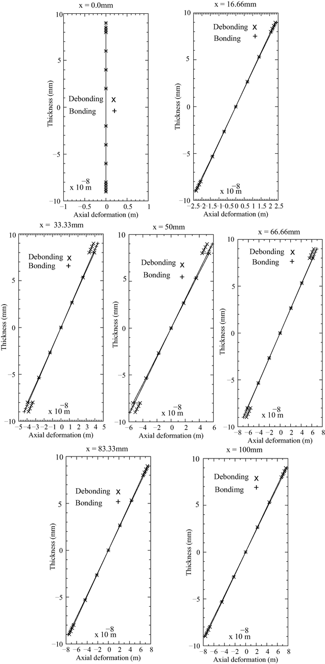
Comparison of Axial Deformation in Bonded and Debonded Beam of 16 mm Core and 1 mm Patch Beam in Sensing.
In case of de-bonded beam, the axial displacement varies along x and z direction (Fig. 3) as it varies in case of fully bonded beam except at de-bonded regions on top and bottom interfaces. The axial displacement for de-bonded case lags from that of axial displacement for bonded case at locations . It can be noticed that the axial displacement lags maximum at the mid span ( ) of the beam at de-bonded interfaces than at the span interfaces and . This is in compliance with the mechanics of stresses that at the de-bonded region, shear stress becomes zero and hence axial deformation of top and bottom patches lags than that of bonded beam case. Further more in the Fig. 3, the antisymmetric behaviour of variation of axial deformation along z direction exhibits proper functioning of the finite element model.
3.1.3 Axial electric field
For the case of fully bonded beam, the axial electric field variation through thickness at the top and bottom surfaces is approximately 20 N/Coulomb at all points on the span,
and
respectively (Fig. 4). Moreover it can be noticed that the electric field variation through thickness is linear.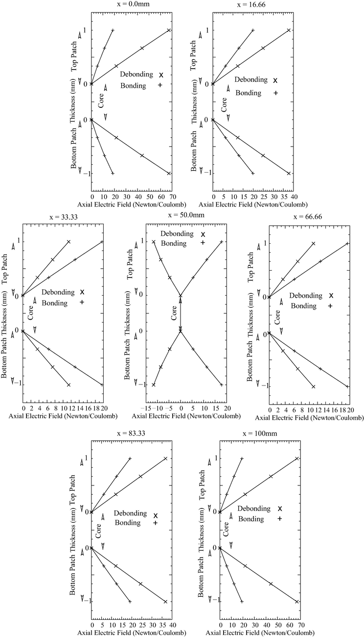
Comparison of Axial Electric Field in Bonded and Debonded Beam of 16 mm Core and 1 mm Patch Beam in Sensing.
For the de-bonded beam as shown in Fig. 1, the variation of axial electric field through thickness has been presented in Fig. 4. It can be noticed that the axial electric field at the top and bottom surfaces at locations along span and . is approximately 67.21 N/Coulomb, 37.68 N/Coulomb, 36.74 N/Coulomb and 66.90 N/Coulomb respectively. The electric field decreases and then increases along span for de-bonded sensing case for the surface locations which correspond to no-debonding. The axial electric field at the de-bonded span on the top and bottom surfaces is 11.38 N/Coulomb, −11.68 N/Coulomb and 10.99 N/Coulomb respectively. The electric field seems remaining constant at the surface points corresponding to de-bonded interfaces. However at the mid span of the beam where the debond is considered, the electric field reverses the direction. Moreover it can be noticed that the magnitude of axial electric field at different locations along span at bonded points in case of de-bonded beam is varying and is high as compared to bonded case. However the magnitude of axial electric field at different locations along span at de-bonded points in case of de-bonded beam is low as compared to bonded case.
3.1.4 Transverse electric field
For the case of fully bonded beam, the transverse electric field variation through thickness at the top and bottom surfaces is found to be as N/Coulomb, N/Coulomb, 0.1362 N/Coulomb, N/Coulomb, N/Coulomb, N/Coulomb and N/Coulomb corresponding to and respectively. It can be noticed that the transverse electric field reduces from root to the tip. Moreover it is found that the electric field variation through thickness is linear.
For the de-bonded beam as shown in Fig. 1, the variation of transverse electric field through thickness has been presented in Fig. 5. It can be noticed that the transverse electric field at the top and bottom surfaces at locations along span
and
is approximately
N/Coulomb, 0.1435
N/Coulomb,
N/Coulomb and −0.03063
N/Coulomb respectively. The electric field decreases along span from root to the tip for de-bonded sensing case for the surface locations which correspond to bonding. The transverse electric field at the de-bonded interface portion of the span locations
and
on the top and bottom surfaces is
N/Coulomb,
N/Coulomb and 0.09685
N/Coulomb respectively. The electric field seems remaining constant at the surface points corresponding to de-bonded interfaces.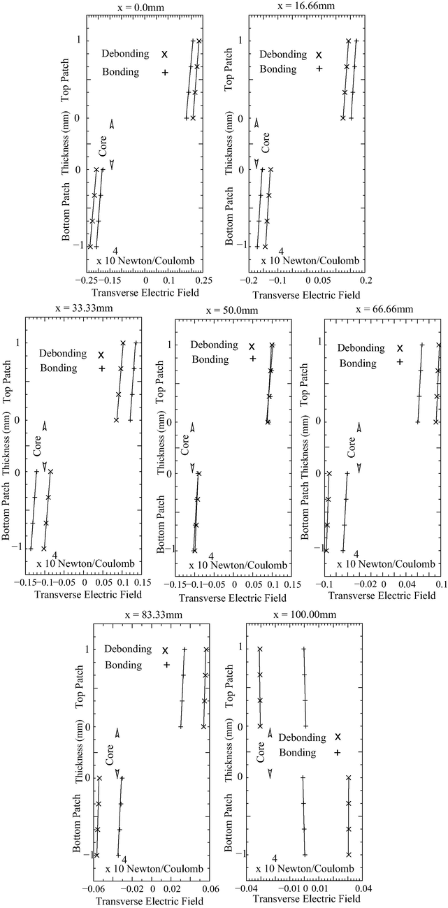
Comparison of Transverse Electric Field in Bonded and Debonded Beam of 16 mm Core and 1 mm Patch Beam in Sensing.
3.1.5 Axial strain
For the case of fully bonded beam, the axial strain through thickness at the span locations
and
on the surface has been presented in Fig. 6 and is found to be
,
,
,
,
,
, and
respectively. This strain seems to be constantly decreasing along span from root to the tip of the smart bonded beam. This is because the bending moment is decreasing from root to the tip. Moreover from the Fig. 6 it can be found that the strain varies linearly through thickness for the bonded beam at the locations
and
. This is because the axial strain is linear function of z-coordinate.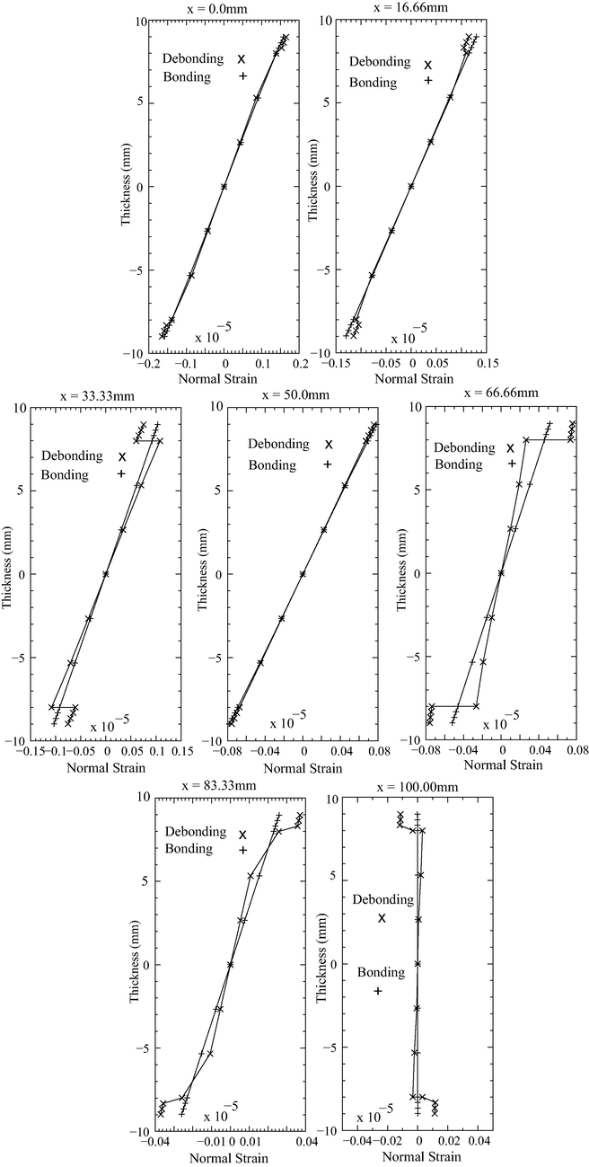
Comparison of Normal Strain in Bonded and Debonded Beam of 16 mm Core and 1 mm Patch Beam in Sensing.
For the de-bonded beam Fig. 1, the axial strain at the locations and on the surface is found to be , , and respectively. This is to be noted that these are the locations where there is no debonding. The strain continuously seems to be reducing from root to the tip in compliance with the bonded beam. The axial strain for the locations is found to be 0.07531 , 0.07560 and 0.07588 at the surface for the de-bonded locations respectively. This strain seems to be remaining constant at the three locations at the surface. It is observed from the Fig. 6, the axial strain through piezo thickness at and leads and lags respectively to that of the axial strain for the bonded case. The axial strain through piezo thickness on the de-bonded portion at and , lags, remains same and leads respectively to that of the axial strain for the case of bonded beam. The axial strain for the de-bonded beam at and , leads and lags respectively to that of the axial strain for the case of bonded beam.
3.1.6 Axial stress
For the case of fully bonded beam, the axial stress through thickness at the span locations
and
on the surface is found to be
,
,
,
,
,
, and −0.00161 Pa respectively. This stress seems to be constantly decreasing along span from root to the tip of the smart bonded beam. It is due to the reason that bending moment decreases from root to the tip. Moreover from the Fig. 7 it can be found that the stress varies linearly through thickness for the bonded beam at the locations
and
except there are jumps at the interfaces. It is due to the reason that material properties of PZT-5H are different from core material. Moreover the normal stress is linear function of the z-coordinate.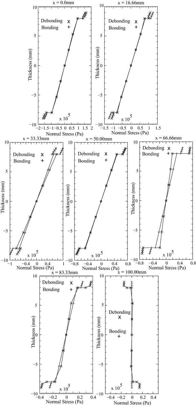
Comparison of Normal Stress in Bonded and Debonded Beam of 16 mm Core and 1 mm Patch Beam in Sensing.
For the de-bonded beam Fig. 1 the axial stress at the locations and on the surface is found to be , , and respectively. This stress continuously seems to be reducing from root to the tip. The axial stress for the locations is found to be , and at the surface for the de-bonded locations respectively. This stress seems to be remaining constant at the three locations at the surface. It is observed from the Fig. 7, the axial stress through piezo thickness at and leads and lags respectively to that of the axial stress for the bonded case. The axial stress through piezo thickness on the de-bonded portion at and , lags, remains same and leads respectively to that of the axial stress for the case of bonded beam. The leading stress is 1.45times than that of the value Of fully bonded stress at the same location i,e . The axial stress for the de-bonded beam at and , leads and lags respectively to that of the axial stress for the case of bonded beam. The disposition of antisymmetric stress across thickness demonstrates the proper functioning of the finite element model. The mechanics involved in debonding being complex therefore the variation in stresses cannot be thoroughly explained. However it can be stated that it is a coupled electro-mechanical behaviour involved with debonding.
3.1.7 Shear strain
For the case of fully bonded beam, the axial strain through thickness at the span locations x = 0.0 mm, x = 16.66 mm, x = 33.33 mm, x = 50.00 mm, x = 66.66 mm, x = 83.33 mm and x = 100.00 mm has been presented in Fig. 8. It can be seen that a constant shear strain equal to
is found to be at the root. This is in accordance with the boundary conditions. Since the term
being non-zero, the strain at the root turns out to be constant. Further at the locations x = 16.66 mm, x = 33.33 mm, x = 50.00 mm, x = 66.66 mm, x = 83.33 mm and x = 100.00 mm, the shear strain is found to be zero at the free surfaces with a kink at the interfaces. It is due to the reason that the finite element model works properly which is exhibited by continuity of shear stresses at the interfaces presented in the Fig. 9. The shear strain is found to be parabolic at all locations except at the root where it is constant. It is because the displacements at the root in longitudinal and transverse directions have been set to zero. Moreover the finite element is based on higher order beam bending in the core as well as in the patches. Therefore the same is exhibited by the results. The maximum shear strain in the core at locations x = 0.0 mm, x = 16.66 mm, x = 33.33 mm, x = 50.00 mm, x = 66.66 mm, x = 83.33 mm and x = 100.00 mm, is found to be
,
,
,
,
,
and
respectively. This strain remains approximately same except at the root. The reason being that the shear force is constant from root to the tip of the cantilever.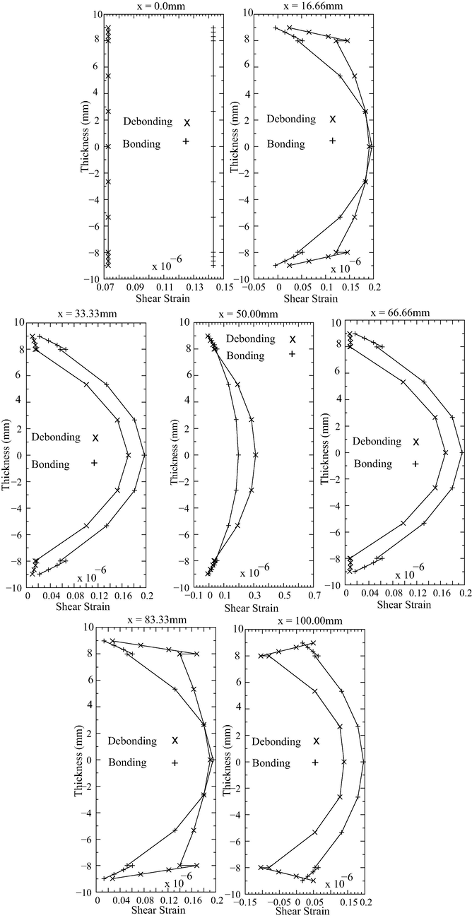
Comparison of Shear Strain in Bonded and Debonded Beam of 16 mm Core and 1 mm Patch Beam in Sensing.
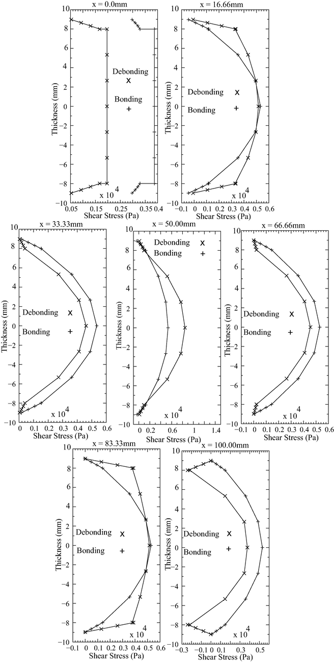
Comparison of Shear Stress in Bonded and Debonded Beam of 16 mm Core and 1 mm Patch Beam in Sensing.
In the case of de-bonded beam Fig. 1 at the locations x = 0.0 mm, x = 16.66 mm, x = 83.33 mm and x = 100.00 mm, the maximum shear strain in the core is , , and respectively. It can be observed that the strain is too low at the root whereas it is higher at all other locations along span. On the left side of the debonding the shear strain increases towards tip whereas on the right side of the debonding the shear strain decreases. Along the debonding locations x = 33.33 mm, x = 50.00 mm, x = 66.66 mm, the maximum shear strain in the core is found to be , and respectively. The trend of the shear strain is that it is maximum at the center of the debonding on the span and is nearly same at the two extremes of the debonding portion. The shear strain is found to be approximately zero at the free surface of the beam as well as on the free interfaces of the debonding portions.
3.1.8 Shear stress
For the case of fully bonded beam, the shear stress through thickness at the span locations, x = 0.0 mm, x = 16.66 mm, x = 33.33 mm, x = 50.00 mm, x = 66.66 mm, x = 83.33 mm and x = 100.00 mm has been presented in Fig. 9. It can be seen that maximum shear stress at the root is equal to . Further at the locations x = 16.66 mm, x = 33.33 mm, x = 50.00 mm, x = 66.66 mm, x = 83.33 mm and x = 100.00 mm, the shear stress is found to be zero at the free surfaces with a kink at the interfaces. This is due to change in the material properties across interface between PZT-5H patch and aluminium core. The shear stress is found to be parabolic at all locations except at the root. It is because the displacements at the root in longitudinal and transverse directions have been set to zero and is non-zero. Moreover the finite element is based on higher order beam bending in the core as well as in the patches therefore the same is exhibited by the results. The maximum shear stress in the core at locations x = 0.0 mm, x = 16.66 mm, x = 33.33 mm, x = 50.00 mm, x = 66.66 mm, x = 83.33 mm and x = 100.00 mm, is found to be , , , , , , respectively. This stress remains approximately same except at the root because shear force is constant from root to the tip. Other than root, the shear stress is found to be continuous at the interfaces. This is due to layer-by-layer finite element model and higher order beam theory which ensures continuity of shear stress at the interfaces.
In the case of de-bonded beam Fig. 1 at the locations x = 0.0 mm, x = 16.66 mm, x = 83.33 mm and x = 100.00 mm, the maximum shear stress in the core is , , and respectively. It can be observed that the stress is too low at the root whereas it is higher at other locations along span other than de-bonded interface portion. On the left side of the debonding the shear stress increases from root onwards whereas on the right side of the debonding, the shear stress decreases towards tip. Along the debonding locations x = 33.33 mm, x = 50.00 mm, x = 66.66 mm, the maximum shear stress in the core is found to be , and respectively. The trend of the shear stress is that it is maximum at the center of the debonding on the span and is nearly same at the two extremes of the debonding portion. The shear stress at the center of the debonding portion is found to be 1.65 times than it was for fully bonded beam corresponding to the same location. Moreover shear stress is found to be approximately zero at the free surface of the beam as well as on the free interfaces of the debonding portions as it is expected to be. This variation of stress from that of the case of fully bonded beam is an electro-mechanical coupling involved with debonding.
In addition to this, shear stress variation at the interfaces and mid layer of the beam along span for fully bonded and de-bonded cases has been presented in Fig. 10 and the results have been presented in Table 2. For fully bonded beam, the shear stresses at the interface start from
at the root and increases immediately to a constant value of
towards the tip at the upper/lower interfaces between patch and the host material respectively. The shear stress at the root at middle of the core starts from 0.39
and varies up to 0.53
at the tip.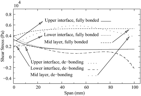
Comparison of Shear Stress along span in Bonded and Debonded Beam of 16 mm Core and 1 mm Patch Beam in Sensing.
Upper
Lower
Upper
Lower
Span
interface
Interface
Mid-layer
interface
Interface
Mid-layer
(mm)
bonding
bonding
Bonding
de-bond
de-bond
de-Bond
00.00
0.3292
0.3870
0.3870
0.16742
0.19681
0.19681
16.66
0.1181
0.1130
0.5325
0.33436
0.32984
0.51698
33.33
0.1515
0.1531
0.5342
0.0(app.)
0.0(app.)
0.46121
50.00
0.1255
0.1226
0.5351
0.0(app.)
0.0(app.)
0.84561
66.66
0.1436
0.1438
0.5300
0.0(app.)
0.0(app.)
0.45518
83.33
0.1395
0.1395
0.5290
0.38722
0.37804
0.51564
100.00
0.1461
0.1463
0.5308
−0.24004
−0.2167
0.37626
For de-bonded beam, the shear stresses at the interface start from at the root and vary sinusoidally to at the tip at the upper/lower interfaces between patch and the host material respectively. The shear stress at the root at middle of the core starts from and varies up to at the tip. The maximum value occurs at middle of the span equal to . This value is larger than fully bonded case value of at the middle of the span. This is important information about the shootup of stresses in de-bonding. The stress analysis shows that the mechanics involved in debonding is complex electro-mechanical coupling.
4 Concluding remarks
The important observations of the study can be summarised as:
-
It is shown that layer-by-layer finite element modeling effectively captures the continuity of shear stress across the interface between piezo-layers and the metallic core.
-
The variation in electric potential, electric field, axial displacement/strain/stress and shear-strain/stress observed in case of debonding demonstrates that the mechanics of debonding is complex coupled electro-mechanical behaviour.
-
Induced potential varies from root to the tip sinusoidally and with reducing trend in case of de-bonded beam at the interfaces and at the free piezo surface. This is attributed to the bending moment varying non-linearly from root to the tip with reducing behaviour in the de-bonded beam.
-
The maximum axial and shear stress due to debonding increases nearly 1.5times to that of the stress in fully bonded beam at various locations.
Acknowledgments
The authors wish to acknowledge Indian Space Research Organisation for their financial support for this research.
References
- Piezoelectricity, An Introduction to the Theory and Applications of Electromechanical Phenomena in Crystals. Vol vol. 1. New York: Dover; 1964.
- Fundamentals of Piezoelectricity. Oxford: Oxford Univ. Press; 1990.
- Non-linear theory of simple micro elastic solid. Int. J. Eng. Sci.. 1964;2(2):189-203.
- [Google Scholar]
- On the Nonlinear Equations of Electro-thermo-elasticity. Int. J. Eng. Sci.. 1971;9(7):587-604.
- [Google Scholar]
- Intelligent structures for aerospace: a technological overview and assessment. AIAA J.. 1994;31(8):1689-1699.
- [Google Scholar]
- A. Chattopadhyay, H. Gu, J. Li. A Coupled Electro-Thermo-elasticity Theory for Smart Composites Under Thermal Load, in: 9th International Conference on Adaptive Structures and Technologies, Technomic, Lancaster, PA, 1998, pp. 156–164.
- Smart beams with extension and thickness-shear piezoelectric actuators. Smart Mater. Struct.. 2000;9(1):1-9.
- [Google Scholar]
- Control of cantilever vibration via structural tailoring and adaptive materials. AIAA J.. 1997;35(8):1309-1315.
- [Google Scholar]
- Use of piezoelectric actuators as elements of intelligent structures. AIAA J.. 1987;25(10):1373-1385.
- [Google Scholar]
- Analysis of beams containing piezoelectric sensors and actuators. Smart Mater. Struct.. 1994;3(4):439-447.
- [Google Scholar]
- New shear actuated smart structure beam finite element. AIAA J.. 1999;37(3):378-383.
- [Google Scholar]
- Analysis of piezoelectrically actuated beams using a layer-wise displacement theory. Comput. Struct.. 1991;41(2):265-279.
- [Google Scholar]
- Finite element analysis of composite structures containing distributed piezoceramic sensors and actuators. AIAA J.. 1992;30(3):772-780.
- [Google Scholar]
- Vibration technique for locating de-lamination in a composite beam. AIAA J.. 1998;36(6):1074-1076.
- [Google Scholar]
- Influence of applied electric field on the energy release rate for cracked PZT/elastic laminates. Smart Mater. Struct. J.. 2001;10:970-978.
- [Google Scholar]
- Finite element analysis of smart structures with piezoelectric sensors/actuators including de-bonding. Chinese J. Aeronaut.. 2004;17(4):246-250.
- [Google Scholar]
- Finite element interface technology for modeling de-lamination growth in composite structures. AIAA J.. 2004;42(6):1252-1260.
- [Google Scholar]
- Linear and non-linear analysis of a smart beam using general electro-thermo-elastic formulation. AIAA J.. 2004;42(4):840-849.
- [Google Scholar]
- Electro-elastic analysis and layer-by-layer modeling of a smart beam. AIAA J.. 2005;43(12):2606-2616.
- [Google Scholar]
- Investigation of de-lamination caused by impact by using a cohesive-layer model. AIAA J.. 2005;43(10):2243-2251.
- [Google Scholar]
- Multiple de-lamination detection of composite beam using magneto-strictive patch. AIAA J.. 2006;44(11):2547-2551.
- [Google Scholar]
- Electro-thermo-elastic formulation for the analysis of smart structures. J. Smart Mater. Struct.. 2006;15:401-416.
- [Google Scholar]
- Thermodynamic modeling of hysteresis effects in piezo ceramics for applications to smart structures. AIAA J.. 2008;46(1):280-284.
- [Google Scholar]
- High frequency dispersion characteristics of smart de-laminated composite beams. J. Intell. Mater. Syst. Struct.. 2009;20:1057-1068.
- [Google Scholar]
- Interaction of the primary anti-symmetric lamb mode (A0) with symmetric de-laminations: numerical and experimental studies. Smart Mater. Struct. J.. 2009;18:1-7.
- [Google Scholar]
- Predicting de-lamination of composite laminates using an imaging approach. Smart Mater. Struct. J.. 2009;18:1-8.
- [Google Scholar]
- Thermal analysis of smart fins in a micro-heat exchanger. Int. J. Nano Biomater.. 2009;2(1/2/3/4/5):12-21.
- [Google Scholar]
- The dynamic behaviour of surface-bonded piezoelectric actuators with de-bonded adhesive layers. J. Acta Mech. 2010;211:215-235.
- [Google Scholar]