

Translate this page into:
Influence of γ-radiation on the physical characteristics of thermally evaporated nanostructured CdS: Cl films
⁎Corresponding author. aman@ksu.edu.sa (Amanullah Fatehmulla)
-
Received: ,
Accepted: ,
This article was originally published by Elsevier and was migrated to Scientific Scholar after the change of Publisher.
Peer review under responsibility of King Saud University.
Abstract
Thermally evaporated CdS: Cl films were subjected to gamma irradiation with an equivalent dose intensity of 4.11 kG/hour for extended periods (60 to 240) minutes. The resultant films were examined by different approaches to acquire structural, morphological and optical information. Upon gamma irradiation doses, the samples show variation in grain size, dislocation density, microstrain and texture coefficient. The XRD patterns exhibit the hexagonal crystal structure formation of CdS: Cl. FESEM images disclosed an extensive spherical nature of nanocrystallites. They demonstrated an increase in their size, while optical study reveals a decrease in bandgap (Eg) and an increase in Urbach energy (EU) due to gamma doses. Electrical studies display a reduction in resistivity upon irradiation doses of gamma. These tailored films can find application as window layers in optoelectronic devices.
Keywords
CdS: Cl
Thermal evaporation
γ-Irradiation
Nanostructured films
Window layers
Optoelectronic devices

1 Introduction
Among the II-VI semiconductor materials, Cadmium sulfide (CdS) is the most promising material possessing creative assets such as direct wide bandgap, small work function, appreciable optical transparency, thermal stability, and electronic charge mobility (Zhai et al., 2007). It has widespread applications in various heterojunction solar cells like copper indium diselenide/sulphide (CIS), copper indium gallium diselenide/sulphide (CIGS), and cadmium telluride (CdTe) (Oladeji et al., 2000; Dobson et al., 2000). It finds applications in different infra-red devices and electro-optic devices that mark it an eye-catching semiconductor (Islam et al., 2013). The properties of semiconductors from II-VI compounds are appreciably valuable with the induced defects and addition of impurities that can be regulated in several ways; for example, gamma irradiation (Ashry and Fayek, 2001; Del Sordo et al., 2009; Capper, 2006; Kasap and Capper, 2017).
CdS films can be prepared using various methods like metal–organic chemical vapour deposition (MOCVD), R.F. sputtering, electro-deposition; pulsed laser ablation, successive ionic layer adsorption and reaction (SILAR), screen printing, chemical bath deposition (CBD), chemical vapour deposition (CVD), thermal evaporation, close space sublimation (CSS), spray pyrolysis, hot wall epitaxy, and molecular beam epitaxy (MBE) (Mahdi et al., 2009; Barreca et al., 2004; Yoon et al., 2006; Amanullah, 2003; Ashour, 2004; Amanullah et al., 2005). Among all the methods, CBD is the prevalent method to deposit thin CdS films for solar cells, and R.F. sputtering technique provides smooth surfaces of CdS thin films. Nevertheless, all the deposition methods significantly affect the physical properties of CdS films. Usually, the non-vacuum coating methods for CdS thin film are prone to oxidation and corrosion; vacuum-built coatings are highly recommended for CdS growth (Hur et al., 2008). Among vacuum-based deposition methods, thermal evaporation is more appropriate to get uniform CdS thin films with the required thickness, pinhole-free and smooth (Memarian et al., 2017).
Generally, the gamma rays can impinge on nanostructured materials by making the atomic displacement in the lattice or creating the ionization (Mokrushin and Tkachev, 1961), and the bond can break due to high radiation dose as well as the atom displaces its position initiating the point defects (Claeys and Simoen, 2002; Kitaev et al., 1965). Consequently, gamma irradiation can alter the features by enhancing or reducing the surface roughness, crystallinity, optical bandgap, photoluminescence, grain resistance, conductivity, and mobility (Khamari et al., 2011) subject to the irradiation dose. Abdel-Galil et al. reported from hydrothermal synthesis the preparation and properties of gamma-irradiated CdS/PVA nanocomposite films and obtained uniformly distributed CdS NPs. With γ doses, their XRD results showed the hexagonal phase of CdS NPs, which spread into the polymeric matrix of polyvinyl alcohol and the enhancement of the average grain size (Abdel-Galil et al., 2020).
Cl doped CdS films have been vacuum deposited at 200 °C substrate temperature using CdCl2 mixed CdS powder (Abu-Safe et al., 2004). The percentage variation of CdCl2 in the mixture ranged from 0 to 20. Substantial variation in carrier mobility, flat band potential, and rise in the concentration of the deep traps were found due to γ-irradiation doses (Atanassova et al., 2001).
The study of the influence of irradiation by gamma rays on the physical characteristics of CdS thin films has received considerable attention in recent years. A specific dose of γ-irradiation increases the activation energy of CdS thin film (Balboul et al., 2016). Gamma irradiation develops a noteworthy tool for changing the material properties by means of its high penetration power (Khatter and Chauhan, 2021).
As of now, no reports exist on the physical properties of gamma-irradiated Cl doped CdS films. However, there is still a great need to carry out the influence of these rays on the physical properties of doped thin films in a broader range of intensities and radiation doses. In the present study, Chlorine doped CdS thin films have been deposited by the thermal evaporation technique on glass substrates. The obtained films have been irradiated with different gamma doses to probe into the structural, morphological, optical and electrical modifications aiming to tailor them for possible optoelectronic applications.
2 Experimental details
2.1 Preparation of CdS and CdS: Cl films
Pure cadmium sulphide thin films were deposited using the Hindhivac coating unit (Model A-12D4) on cleaned substrates of glass by evaporating 99.999% pure CdS powder kept in a molybdenum boat at a vacuum of 5 × 10⁻⁶ torr. The substrates were kept at 200 0C, and the source to substrate height was 14 cm. The deposition rate was maintained at 7 Å/sec. The doped CdS films were coated onto the substrates by electrically heating 99.99% CdCl2 mixed with 99.999% CdS powder placed in a molybdenum boat. Since CdCl2 and CdS have comparable vapour pressures at elevated temperatures (845 0C), it was likely that the films would likely have identical vapour pressure on the substrates when the mixture is heated steadily. The boat had CdS powder mixed with 20% CdCl2 by mass calculated from the per cent composition relation (Murt and Guldner, 1969):
The mixture was positioned in the evaporation unit, and the vacuum chamber was reduced to 5 × 10⁻⁶ torr. The source current was raised steadily till 90 A to confirm the uniform temperature in the evaporating mixture while the substrate temperature was maintained constant at 200 °C. The evaporation of the mixture started at 840 °C. As the film thickness touched 1000 Å, the shutter was closed for evaporation and reduced the source current gradually to zero. The rate of deposition was maintained at 7 Å/sec.
2.2 Gamma (γ) irradiation
We studied the phenomenon of changes in the physical properties of these films. The deposited pure and 0.2 wt% chlorine doped CdS films were irradiated by gamma irradiation with an equivalent intensity to 4.11 kG/hour for extended periods of 60 min, 120 min, 180 min, and 240 min, respectively. This gamma cell is loaded with source No. GS-415, which contains 24,910 Ci of Cobalt-60 as slugs in 16 pencils. The chamber’s centre’s dose rate was obtained by ferrous sulphate dosimetry according to quality control specification QC-16-3511. The accuracy of the assessed dose rate is at the 95% assurance limit.
2.3 Characterization techniques
The prepared and gamma-irradiated nanostructured CdS: Cl films were characterized using XRD, FESEM, UV–Vis-NIR, and two electrical probe techniques. XRD studies were carried out using X pert- Pro MRD system from PANalytical, Netherlands. The tension and current for the X-ray tube were 45KV & 40 mA, respectively. The surface feature of the samples was analyzed using JSM-7600F, JEOL Scanning Electron Microscope. Optical transmittance (T) studies were made in the 200–3100 nm wavelength range with a UV–VIS-NIR spectrophotometer (Cary 5000 from varian). D.C. resistivity measurement was done using two probes I-V measurement technique.
3 Results and discussion
3.1 Sample preparation
CdS: Cl thin films were deposited on 75 mm × 25 mm glass substrates in the present investigation. The prepared Chlorine doped Cadmium sulfide thin films were divided into 6 mm × 6 mm square samples using a diamond cutter. These samples were subjected to gamma irradiation with an equivalent dose intensity of 4.11kG/hour for an extended (60 to 240) minute, as described in Table 1.
Sample
Gamma Irradiation time
Gamma Doses (kG/h)
CS (pure)
Without irradiation
0
CS1
60 min
4.11
CS2
120 min
8.22
CS3
180 min
12.33
CS4
240 min
16.44
3.2 Structural investigation
CdS: Cl thin films’ crystalline structure was examined by XRD analysis at room temperature.
In the CdS hexagonal structure (
), the d spacing is obtained using the relation (Cullity and Stock, 2001):
The calculated lattice parameters match well with the PDF file # 6 – 0314 for CdS, as shown in Table 2.
Material
Calculated
PDF # 6-0314
a(Å)
b(Å)
c(Å)
a(Å)
b(Å)
c(Å)
CdS
4.147 Å
4.147 Å
6.721 Å
4.136 Å
4.136 Å
6.713 Å
From Fig. 1, it can be seen that there are nine peaks (0 0 1), (2 1 0), (1 0 0), (1 1 1), (0 0 2), (1 0 2), (1 1 2), (1 1 0), and (1 1 2) in the pattern. All the characteristic peaks of as-deposited films belong to the wurtzite structure of CdS. For the pure and γ-irradiated samples, the peaks (0 0 1)H and (1 1 2)H belong to the Hexagonal phase of Cd(ClO4)26H2O material [card no. 14-24]. It may be due to the precursor used for doping Chlorine in CdS. The γ-irradiated films exhibit (2 1 0) & (3 3 0) peaks that belong to the orthorhombic phase of CdCl2. Although most of the peaks belong to the Hexagonal phase of CdS [card no.6-0314], the effect of irradiation may be considered for the films to have a bit mixed phase. The preferentially oriented peak is (0 0 2). Also, the intensity of orientation peaks (0 0 2), (1 0 2) and (1 1 0) increased with increasing irradiation dose from 60 min to 180 min, while the peak intensity decreased for 240 min. It is attributed to the induced defects by γ irradiation, resulting in the scattering of x-ray with no alteration in the crystal structure (Ali et al., 2020a). The structural calculations for each of these peaks are shown in Tables 3, 4 and 5. The structural parameters like D- average crystallite size, Ɛ- microstrain, δ- dislocation density, L-bond length and TC- the texture coefficient of the CdS: Cl films were obtained by using the formulae (Ejderha et al., 2010).
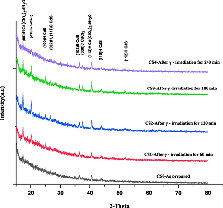
XRD analysis of CdS: Cl films irradiated by various gamma doses.
Sample
θ
β = FWHM
(nm)
hkl
L(Å)
TC
CS pure
13.280
0.22
37.101
0.00934
3.353
002
0.000726
1.679
0.593
CS1
13.255
0.19
42.955
0.00806
3.359
002
0.000541
1.679
0.756
CS2
13.245
0.17
48.006
0.00722
3.361
002
0.000433
1.680
0.671
CS3
13.245
0.16
51.007
0.00679
3.361
002
0.000384
1.680
0.555
CS4
13.290
0.15
54.417
0.00636
3.350
002
0.000376
1.680
0.626
Sample
θ
β = FWHM
(nm)
hkl
(nm)-2
L(Å)
TC
CS pure
18.245
0.25
33.458
0.00103
2.460
102
0.000893
1.843
0.738
CS1
18.205
0.18
46.459
0.00746
2.465
102
0.000463
1.843
0.484
CS2
18.225
0.16
52.272
0.00663
2.462
102
0.000365
1.279
0.780
CS3
18.230
0.15
55.759
0.00621
2.462
102
0.000321
1.279
0.951
CS4
18.230
0.10
83.638
0.00414
2.462
102
0.000142
1.279
0.957
Sample
θ
β = FWHM
(nm)
hkl
(nm)-2
L(Å)
TC
CS pure
21.845
0.30
28.528
0.00121
2.070
110
0.00122
1.951
0.504
CS1
21.910
0.26
32.932
0.00105
2.064
110
0.00092
1.951
0.447
CS2
21.885
0.25
34.244
0.00101
2.066
110
0.00085
2.160
0.348
CS3
21.875
0.17
50.355
0.00068
2.067
110
0.00039
2.160
0.402
CS4
21.865
0.16
53.499
0.00064
2.068
110
0.00034
1.951
0.514
The lower FWHM and significant D values indicated appreciable crystallization of thin films. It can be seen from Tables (3, 4 and 5) that by increasing the gamma irradiation time, the FWHM values decreased slightly, and the grain size values increased. It is due to film recrystallization as a result of γ-irradiation. XRD studies revealed improved crystallinity of these films. The microstrain as well as β exhibit decreasing trend. Also, it can be noted from Tables 3, 4 and 5 that the dislocation density and the grain size exhibit an inverse relationship. Similar observations were reported for CdS films prepared by thermal evaporation (Ali et al., 2019).
The bond length
is given by the formula (Barret and Massalski, 1980):
Where the parameter u in the hexagonal structure given by:
From Tables 3, 4 and 5, it can be seen that low irradiation dose does not influence L (A). However, with higher irradiation doses, one can observe high and low L(A) values for (1 1 0) orientation peaks. In contrast, the opposite trend for the (1 0 2) orientation peak is noticed. It may be ascribed to the variance in the atomic radius of cadmium and chlorine.
The texture coefficient that provides the quantitative information of the crystal preferential orientation is given by (Pankove, 1971):
Here, the texture coefficient is TC (hkl), the XRD intensity represents I(hkl), and n stands for the amount of diffracted peaks considered. Io(hkl) denotes the reference XRD intensity for the randomly oriented particles. If TC (hkl) = 1, it is believed that the films have crystallites with random orientation (JCPDS file # 36-1451, 2001, ASTM, 1966), whereas the values greater than 1 designate the plenty of particles in a particular (hkl) track. If the TC values lie between 0 < TC (hkl) < 1, it infers the deficiency of particles oriented in that track. As TC (hkl) exhibits an increasing trend, the preferred growth of grains perpendicular to the hkl plane direction becomes more significant. The TC variations are shown in Tables 3, 4 and 5. The largest TC can be observed in the (1 0 2) plane. The values of TC (1 0 2) display an increasing tendency with the increase of doses up to 180 min irradiation. However, there is a steep fall in TC with 240 min irradiation time.
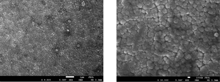
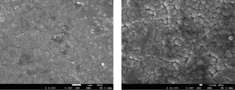
3.3 Surface morphology
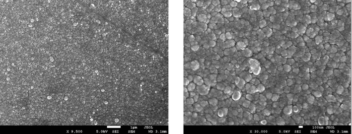
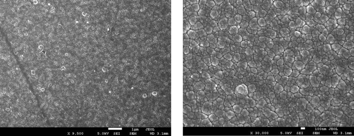
Surface morphology analysis has been carried out using FESEM for pure and γ irradiated (CdS)0.8Cl0.2 films.
From Figs. 2(a) to 2(e), it can be observed that low (9500x) and high (30,000x) magnification images of the said samples. Except for the pure sample, one can notice that the irradiated samples exhibit large spherical crystallite sizes of varying degrees. Additionally, for 2(b) to 2(e) SEM images, ImageJ software has been used to draw grain size plots, and it gives clear insight into the change in grain size along with gamma rays’ time duration. The grain size appears to increase with irradiation time, which is in line with XRD analysis. Upon increase of γ irradiation dose, a large amount of energy is transmitted to the CdS: Cl lattice in a short duration and transformed into the kinetic energy that could be the reason for the collection of particles thermal eruptions through which the small particle develops into a cluster of grains (Abhirami et al., 2013).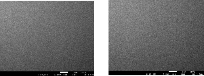
SEM image for CdS: Cl pure before γ irradiation (0 min).
SEM image for CdS: Cl after γ irradiation (60 min).
SEM image for CdS: Cl after γ irradiation (120 min).
SEM image for CdS: Cl after γ irradiation (180 min).
SEM image for CdS: Cl after γ irradiation (240 min)
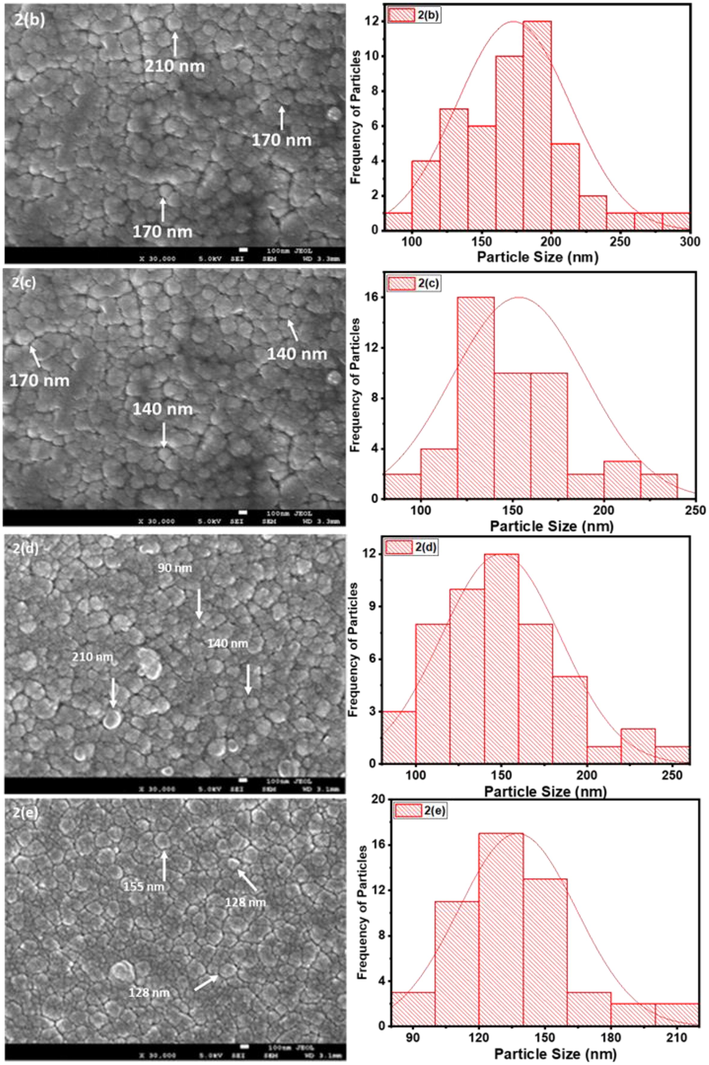
(b) to (e). SEM images and particle size distribution for CdS: Cl after γ irradiation.
3.4 Optical properties
Fig. 3 shows the transmission spectra of gamma-irradiated CdS: Cl thin films.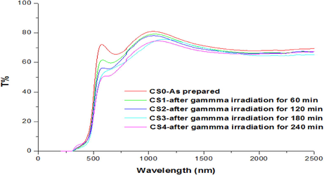
Comparison of transmission spectra of CdS: Cl films subjected to gamma doses.
Absorption coefficient α is obtained using Lambert’s law (Joseph et al., 2006).
It can be observed that; at wavelengths (λ < 380 nm), the absorbance is high, whereas at wavelengths (λ > 380 nm), the absorbance is low (Alarcón et al., 2011). The film performed as an opaque material with its significant absorbing characteristics at small wavelengths and as a transparent material at extended wavelengths. CdS: Cl film displays appreciable average transmittance (∼ 73:9%) in the optical region. Hence, the obtained film represents an admirable optical quality (Li et al., 2005). From the figure, it can be noticed that the transmission drops with the rise in gamma irradiation doses in all the films. The slight decrease in transmission after irradiation may be due to an enhancement in the particle size of these films. Also, the transmission curve creeps towards the red wavelength when the gamma irradiation dose increases. As shown in Fig. 3, all the samples exhibit a steep fall in transmission at the fundamental band edge absorption. The energy bandgap can be deduced from the parabolic bands and the Tauc model (Yakuphanoglu et al., 2004):
Figs. 4 and 5 illustrate the change of energy bandgap with gamma doses. Fig. 5 shows that the energy band gap decreases with the increase of gamma doses and is attributed to increased defects or structural disorders in the films (Khatter and Chauhan, 2021).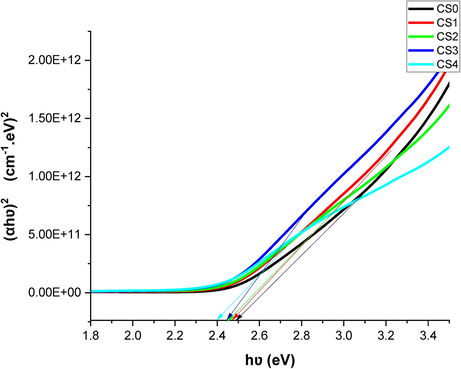
Tauc’s plots for the as-prepared and γ -irradiated CdS: Cl films.
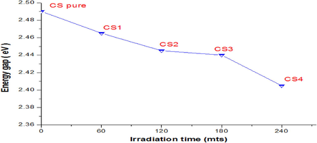
Energy gap (Eg) variation for the CdS: Cl samples with gamma irradiation doses.
The absorption coefficient α close to the band edge demonstrates exponential dependency on hν-the photon energy (Tauc, 2012):
In Eq. (10), EU denotes the Urbach energy corresponding to the width of the band tail, αo, EI are the constants. So, the ln(α) versus hν plot ought to be linear, and EU can be obtained from the slope. The calculated EU values are listed in Table 6.
sample
Gamma Doses
(kG/h)
Eg (eV)
Eu (meV)
β (×10−3)
C.S. pure
0
2.490
1.667
15.511
CS1
4.11
2.465
1.786
14.477
CS2
8.22
2.445
2.500
10.340
CS3
12.33
2.440
2.272
11.374
CS4
16.44
2.405
5.000
5.170
EU values show an increasing behavior with the decrease in the energy gap.
As the localized states and the electronic transition between them deduce the dependence of α with hν, the density of states drops off exponentially with photon energy. This behavior is consistent with Tauc’s theory. So, the Eq. (10) can be re-arranged as (Tauc, 2012):
Here, β is the steepness parameter, which portrays the broadening of absorption edge because of exciton–phonon interaction or electron–phonon interaction. If the slope in Eq. (10) is related to the width of edge, the parameter
can be written as.
The obtained β values at room temperature are shown in Table 6. The steepness parameter decreases with a decrease of the energy gap, and the Urbach energy shows increasing behavior (Fig. 6). The advent of the Urbach tail is accredited to structural disorder triggered by defects and doping in films.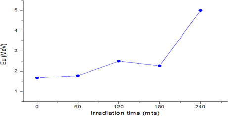
Illustration of
versus gamma doses on CdS: Cl films.
3.5 Electrical properties
The resistivity of thin films can be calculated using.
By measuring the impact resistance of thin films with irradiation doses, we found a significant change in the resistivity for all samples. We note that with the rising irradiation dose, the resistivity of the films decreased in an inverse relationship, where we note that the resistivity decrease substantially when measured directly after irradiation (Balboul et al., 2016). Later, we also noticed that the resistivity gradually showed an increasing trend with passage of time as shown in Fig. 7 as well as Table 7. Conversely, the resistivity value increased with an increase in the dose level of gamma exposure. This might be due to an increase in the grain size with the gamma exposure dose. Also, associated with induced-defect density and the charge transportation in grain boundaries (Ali et al., 2020b; Tawfik et al., 2022).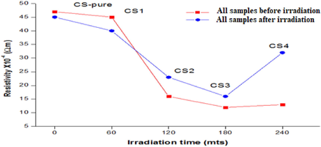
Resistivity variation of CdS: Cl films with irradiated gamma doses.
sample
Gamma Doses
(kG/h)
Resistivity KΩ
Before irradiation
Immediately After irradiation
CS1
4.11
45
40
CS2
8.22
16
23
CS3
12.33
12
16
CS4
16.44
13
32
4 Conclusions
The influence of γ- irradiation doses on the Nanostructured CdS0.8Cl0.2 films prepared by thermal evaporation technique resulted in hexagonal wurtzite crystal structure with an increase in grain size of the films and decrease in dislocation density. FESEM images revealed the sizeable spherical nature of crystallites and increased their size with tight cluster formations. Transmission of the films increased, and the band edge exhibited redshift. Optical band bandgap values decreased. The steepness parameter decreased with the decrease of the energy gap, and the Urbach energy showed increasing behavior. Resistivity decreased, but with ageing, it is noted that the resistivity gradually showed an increasing trend. Band gap engineering demonstrates that the CdS:Cl films find application as window layers in optoelectronic devices. The perceptible variations induced in the structural, optical, and electrical properties of CdS: Cl films clearly present the prospect of using them in gamma dosimetry application.
Acknowledgements
The authors would like to thank the Researchers Supporting Project, RSP-2021/42, King Saud University, Riyadh, Saudi Arabia, for the financial support.
Declaration of Competing Interest
The authors declare that they have no known competing financial interests or personal relationships that could have appeared to influence the work reported in this paper.
References
- Synthesis and Characterization of γ- Irradiated Cadmium Sulfide/Polyvinyl Alcohol Nanocomposites Films. J. Electron. Mater.. 2020;49(3):2222-2232.
- [Google Scholar]
- Effect of SHI irradiation on the morphology of SnO2 thin film prepared by reactive thermal evaporation. Vacuum. 2013;90:39-43.
- [Google Scholar]
- Chlorine- doped CdS thin films from CdCl2-mixed CdS powder. J. Electron. Mater.. 2004;33(2):128-134.
- [Google Scholar]
- Effect of γ-irradiation on the growth of ZnO nanorod films for photocatalytic disinfection of contaminated water. J. Colloid Interface Sci.. 2011;364(1):49-55.
- [Google Scholar]
- Gamma dose-dependent structural, optical and current-voltage characteristics of CdS/p-Si heterojunction. Mater. Chem. Phys.. 2020;240:122243.
- [Google Scholar]
- Investigation of gamma irradiation effects on the properties of CdS/p-Si heterostructure. Mater. Sci. Semicond. Process.. 2019;93:44-49.
- [Google Scholar]
- Influence of gamma irradiation on the properties of PbS thin films. Radiat. Phys. Chem.. 2020;171:108732.
- [Google Scholar]
- Effect of isochronal annealing on CdTe and the study of electrical properties of Au CdTe Schottky devices. Can. J. Phys.. 2003;81(3):617-624.
- [Google Scholar]
- Co-activation effect of Chlorine on the physical properties of CdS thin films prepared by CBD technique for photovoltaic applications. Physica status solidi (a). 2005;202(13):2474-2478.
- [Google Scholar]
- Physical properties of spray pyrolyzed CdS thin films. Turk. J. Phys.. 2004;27(6):551-558.
- [Google Scholar]
- Radiation effects on fabricated Cu2S/CdS heterojunction photovoltaic cells. Renew. Energy. 2001;23(3–4):441-450.
- [Google Scholar]
- Influence of γ radiation on thin Ta2O5–Si structures. Microelectron. J.. 2001;32(7):553-562.
- [Google Scholar]
- Electrical Response of CdS Thin Film and CdS/Si Heterojunction to Gamma Radiation. Adv. Mater. Sci. Eng.. 2016;2016:1-7.
- [Google Scholar]
- CVD of Nanophasic (Zn, Cd) S Thin Films: From Multi-Layers to Solid Solutions. Chem. Vapor Deposition. 2004;10(4):229-236.
- [Google Scholar]
- Barret, C.S., Massalski, T.B., 1980. Structure of Metals. Pergamon Press.
- Capper P., ed. Springer handbook of electronic and photonic materials. New York: Springer; 2006.
- Radiation effects in advanced semiconductor materials and devices. Vol Vol. 57. Springer Science & Business Media; 2002.
- Elements of x-ray diffraction. Upper Saddle River, NJ: Prentice-Hall; 2001. p. :388.
- Progress in the development of CdTe and CdZnTe semiconductor radiation detectors for astrophysical and medical applications. Sensors. 2009;9(5):3491-3526.
- [Google Scholar]
- Stability of CdTe/CdS thin- film solar cells. Sol. Energy Mater. Sol. Cells. 2000;62(3):295-325.
- [Google Scholar]
- Ejderha, K., Yıldırım, N., Türüt, A.B.D.U.L.M.E.C.İ.T., Abay, B., 2010. Influence of interface states on the temperature dependence and current-voltage characteristics of Ni/p-InP Schottky diodes. Superlatt. Microstruct., 47(2), 241-252.
- Characterization of photoconductive CdS thin films prepared on glass substrates for photoconductive- sensor applications. J. Vacuum Sci. Technol. B: Microelectron. Nanometer Struct. Process. Measur. Phenomena. 2008;26(4):1334-1337.
- [Google Scholar]
- Comparison of structural and optical properties of CdS thin films grown by CSVT, CBD and sputtering techniques. Energy Procedia. 2013;33:203-213.
- [Google Scholar]
- Studies on the structural, electrical and optical properties of Al-doped ZnO thin films prepared by chemical spray deposition. Ceram. Int.. 2006;32(5):487-493.
- [Google Scholar]
- Kasap, S., Capper, P. (Eds.), 2017. Springer handbook of electronic and photonic materials. Springer.
- Effect of 60Co γ-ray irradiation on electrical properties of GaAs epilayer and GaAs p–i–n diode. Nucl. Instrum. Methods Phys. Res., Sect. B. 2011;269(3):272-276.
- [Google Scholar]
- Gamma-ray induced modifications on CdS nanorod mesh: Structural, optical, and electrical properties. Radiat. Phys. Chem.. 2021;182:109353.
- [Google Scholar]
- Conditions for the chemical deposition of thin cadmium sulphide films on a solid surface. Russ. J. Phys. Chem.. 1965;39:1101-1102.
- [Google Scholar]
- On the origin of blue-green luminescence in spray pyrolyzed ZnO thin films. J. Mater. Sci.. 2007;42(8):2598-2602.
- [Google Scholar]
- Zinc oxide films by thermal oxidation of zinc thin films. Surf. Coat. Technol.. 2005;198(1–3):319-323.
- [Google Scholar]
- Mahdi, M.A., Kasem, S.J., Hassen, J.J., Swadi, A.A., A l-Ani, S.K.J., 2009. Structural and optical properties of chemical deposition CdS thin films.
- Deposition of nanostructured CdS thin films by thermal evaporation method: Effect of substrate temperature. Materials. 2017;10(7):773.
- [Google Scholar]
- Mokrushin, S.C., Tkachev, Y.D., 1961. Kolloid Zh. 23 (1961) 438. Colloid J.(USSR), 23, 366.
- Murt E.M., Guldner W.G., eds. Physical Measurement and Analysis of Thin Films. Boston, MA: Springer US; 1969.
- Metal/CdTe/CdS/Cd1− xZnxS/TCO/glass: A new CdTe thin-film solar cell structure. Sol. Energy Mater. Sol. Cells. 2000;61(2):203-211.
- [Google Scholar]
- Pankove, J.I., 1971. Optical processes in semiconductors Prentice-Hall. New Jersey, 92.
- Monolayer Graphene Radiation Sensor with Backend RF Ring Oscillator Transducer. Nanomaterials. 2022;12(3):305.
- [Google Scholar]
- Tauc, J. (Ed.), 2012. Amorphous and liquid semiconductors. Springer Science & Business Media.
- The determination of the optical constants of Cu (II) compound having 1-chloro-2, 3-o-cyclohexylidinepropane thin film. Opt. Commun.. 2004;239(4–6):275-280.
- [Google Scholar]
- Preparation of CdS thin films through MOCVD method, using Cd-S single-source precursors. Bull. Korean Chem. Soc.. 2006;27(12):2071-2073.
- [Google Scholar]
- Design and fabrication of rocketlike tetrapodal CdS nanorods by seed-epitaxial metal-organic chemical vapour deposition. Cryst. Growth Des.. 2007;7(3):488-491.
- [Google Scholar]