

Translate this page into:
Gamma ray-induced effects on the properties of CsPbBr3 perovskite thin film
⁎Corresponding author. sdawood@ksu.edu.sa (S. Aldawood)
-
Received: ,
Accepted: ,
This article was originally published by Elsevier and was migrated to Scientific Scholar after the change of Publisher.
Peer review under responsibility of King Saud University.
Abstract
In the last two decades, the family of metal halide perovskites has received more attention in radiation detection applications. In this work, the radiation detection and dosimetric applicability of the CsPbBr3 thin film will be investigated. The impact of gamma irradiation on the structural, morphological, optical, and electrical properties of the CsPbBr3 thin film has been studied. The CsPbBr3 thin film was synthesized using a thermal evaporation deposition technique. The deposited thin films were exposed to different gamma-ray doses (0, 25, 50, 75, and 100 kGy) using a 60Co gamma source with an activity of 7.328 kGy/h. X-ray diffraction analysis of the thin films confirmed the orthorhombic crystal structure and also showed an increase in the crystalline and crystallite sizes, whereas the dislocation density and microstrain decreased as the gamma dose increased. Field-emission scanning electron microscopy results revealed that the surface morphology changed considerably due to gamma exposure. The optical properties exhibited a decreasing energy band gap value (from 2.35 to 2.14 eV) as the radiation dosage increased, which may have been due to the increasing crystallite size and induced defects. The photoluminescence (PL) peaks shifted toward longer wavelengths and intensity, while the full width half maxima of PL peaks increased along with the gamma dose, which was attributed to spectral broadening and enhancement in the recombination rate of electron–hole pairs. Impedance spectroscopy of all the irradiated samples showed the single semicircle feature, which is similar to that observed in the case of unirradiated samples. The grain boundary resistance reduced gradually as the gamma dosage increased. The achieved outcomes proved that the structural defects induced by gamma exposure had a superficial influence on the structural, morphological, optical, PL, and impedance properties of CsPbBr3 thin films. The impact of gamma dose on the properties makes CsPbBr3 thin films significantly useful as sensing materials.
Keywords
Metal halide CsPbBr3 perovskite thin films
Gamma irradiation
XRD
Optical properties
Photoluminescence
Impedance spectroscopy

1 Introduction
Due to high penetration, gamma irradiations are crucial for changing the structural, optical, electrical, and mechanical properties of thin films (Güllü et al., 2008). Gamma irradiations produce temporary or permanent modifications in thin film characteristics as a function of dose (Ocak et al., 2010; Tuğluoğlu et al., 2015). High-energy radiation sensing can be applied directly or indirectly. In a direct method, high-energy photons interact with materials and directly create a pair of charges that can be separated by electrodes. Indirect methods involve high-energy radiation primarily changing into light via scintillating materials; afterward, it is transformed to an electrical signal by a photo sensor. The direct technique adopts the improvements of high sensitivity, room temperature, and low cost active matrices based on nanostructure and unique material (such as inorganic semiconductors) (Starkenburg et al., 2017). Currently, inorganic metal halide perovskites have attained considerable interest in many fields of science and technology because of their low manufacturing costs and extraordinary structural, optical, electrical, and mechanical properties (Zhang et al., 2016). In the last decade, the family of metal halide perovskites has been comprised of the profound structural formula ABX3, where A is generally organic/inorganic cation, B is a metal cation and the X site establishes anion (halogens; e.g., A is CH3NH3+ (MA+), HN = CHNH3+ (FA+), Rb+, Cu+, Cs+, and Li+; B is Sn2+, Ge2+, and Pb2+; and X = I-, Br-, and Cl-), which has attained widespread attention (Li et al., 2020; Popoola, 2020) due to its outstanding performance in solar cells (Zhu and Zhu, 2020), Li-ion batteries (Kostopoulou et al., 2019), super capacitors (Xu et al., 2015), light emitting diodes (Nair and Dhoble, 2020), photo detectors, and lasers (Shi and Jayatissa, 2018; Wei and Huang, 2019). Hany et al. explored the optical and electrical properties of TlPbI3 single crystals by using UV–IR absorption spectroscopy, low temperature cathodoluminescent, charge carrier mobility lifetime measurements, and current–voltage characteristics (Hany, 2021). Chung et al. investigated the unique features of CsPbI3 (such as its high-electrical conductivity and good photoluminescence (PL)) and also noted its band gap (1.3 eV), electron mobility (585 cm2 V−1), and carrier concentration at room temperature (1017 cm−3) (Chung et al., 2012). He et al. reported that CsPbBr3 is an exceptional halide perovskite material for the detection of gamma rays with 57Co and 137Cs, recording its mobility lifetime (1.34 × 10⁻³ cm2 V−1) and hole carrier lifetime (25 µs) (He, 2018). Cesium lead tribromide (CsPbBr3) is a significant inorganic halide perovskite that has attained considerable attention due to its unique structural, optical, electrical, and mechanical properties as a sensing material (Qian et al., 2016). Exclusively, there have been remarkable research efforts toward the expansion of perovskite materials for gas sensing applications and further research progress is desired (Ahmadi et al., 2017). Using halide perovskites for sensing elements has shown much better results than the conventional metal oxide gas sensors due to the former’s ability to operate at a high temperature and with partial resistivity (Kymakis et al., 2020; Moseley, 2017).
Different deposition techniques have been reported (e.g., the sol–gel method, coprecipitation method, solution method, radio frequency sputtering, chemical bath deposition, pulse laser deposition, electron beam evaporation, and thermal evaporation) for the production of thin films (Ali, 2017). Among these, the thermal evaporation method is superior to others due to many integrated advantages (e.g., clean, less expensive, solvent free, and low processing temperature). Gamma irradiation is believed to possess the capability to shuffle host material atoms from their lattices. This observable fact is responsible for initiating nanostructure deviation; the alterations produced by gamma irradiation depends on the dosage, interaction angle, and nature of host materials (Ivanov and Platov, 2004). Nanomaterial interactions with gamma radiation exhibit the creation of defects in the form of clusters, deficiencies, and dislocations (Kanazawa and Adachi, 1998). These cluster defects exhibit the energy levels in the energy band gap, which can act as carrier trapping or carrier recombination centers that associate with energy (Atanassova et al., 2001; Chakrabartty, 2014). The novelty of the present study is to investigate the different effects of gamma dosages on the properties of the CsPbBr3 thin films, deposited by thermal evaporation. This includes the full analysis of the structural, morphological, optical, and electrical properties as a function of gamma doses, in order to investigate the applicability the CsPbBr3 thin films for radiation dosimetry and sensing applications.
2 Materials and methodology
2.1 Deposition of CsPbBr3 thin film
The CsPbBr3 thin film was prepared using thermal evaporation. Glass substrates were washed using detergent placed in an ultra-sonication bath before starting deposition; the bath was followed by acetone, ethanol, and deionized water treatments for about 30 min each. In the first step, the CsPbBr3 thin film, CsBr, and PbBr2 had a 1:1 M ratio before being loaded into a single boat inside the thermal evaporation system vacuum chamber. In the second step, the glass substrates were placed in a holder facing toward the sources. To allow evaporation, evaporator chamber pressure was reduced to 10−4 mbar and the material was transferred to the substrates using only a small number of collisions with ambient gas molecules. Subsequently, two precursors were evaporated together via raising the tungsten boat current. The prepared thin films were then exposed to different gamma doses (0, 25, 50, 75, and 100 kGy) by using a 60Co gamma source. The gamma exposure procedure, applied on CsPbBr3 thin film, was carried out in National Center for Irradiation Technology, King Abdulaziz City for Science & Technology using Co60 (energy = 1.31 MeV and activity = 7.328 kGy/h) source in close chamber (Model SC220E, MDS Nordion).
2.2 Structural measurements
The structural parameters, such as crystalline size (D), microstrain (ε), and dislocation density (δ), of pristine and gamma-irradiated CsPbBr3 thin films were calculated using the Debye–Scherer formula (Ali, 2017):
The lattice constant a, b and c of the orthorhombic structure was determined using Miller indices of the (0 2 2), (2 0 2) and (3 0 1) peaks.
2.3 Optical measurement
To determine the band gap value Eg, the absorption coefficient α is calculated by performing equations (6), (7), and (8) (Yakuphanoglu et al., 2009; Urbach, 1953):
2.4 Electrical measurement
The dc conductivity (σdc) across the grain boundaries was determined from the grain boundary resistance by using the given relation
2.5 Characterization
The X-ray diffraction (XRD) analysis of CsPbBr3 thin film was observed by using an X-ray diffractometer (Panalytical XPert3MRD X) with a Cu-Kα (λ = 1.54 Ǻ) source of radiation. The surface morphology of the thin film was examined by using a field-emission scanning electron microscope (FESEM; JEOL). The optical properties were measured on an ultraviolet–visible light spectrophotometer (JASCO-V 670) and PL spectra were recorded on a spectrometer (JESCO FP-8200). In addition, the impedance spectroscopy was examined with a frequency analyzer (hioki-3570) at room temperature running ZView software.
3 Results and discussion
3.1 Structural investigation
The XRD pattern of the CsPbBr3 gamma irradiation with doses ranging from 0 to 100 kGy, as shown in Fig. 1, had peaks of (1 0 0), (1 1 0), (1 1 1), (2 0 0), (2 1 0), (2 1 1), and (2 2 0) positioned at 14.96, 21.40, 25.22, 30.32, 34.04, 37.59, and 43.77, respectively, which indicate the crystalline nature of the thin film. All the peaks in the XRD pattern are in consensus [JCPDS 05_0592], confirming the orthorhombic perovskite phase structure. Ghaithan et al. reported the same structural phase of CsPbBr3 thin films prepared by thermal evaporation at room temperature (Ghaithan et al., 2021). With an increase in gamma dosage, various modifications were observed on the CsPbBr3 crystal structure. Among all peaks, the (2 0 0) peak was the main peak and its intensity increased with increasing gamma dosages (0–100 kGy), as shown in Fig. 2-a. It can also be seen very clearly that all samples were crystalline in nature.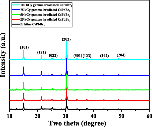
XRD patterns of CsPbBr3 thin film with different gamma doses.
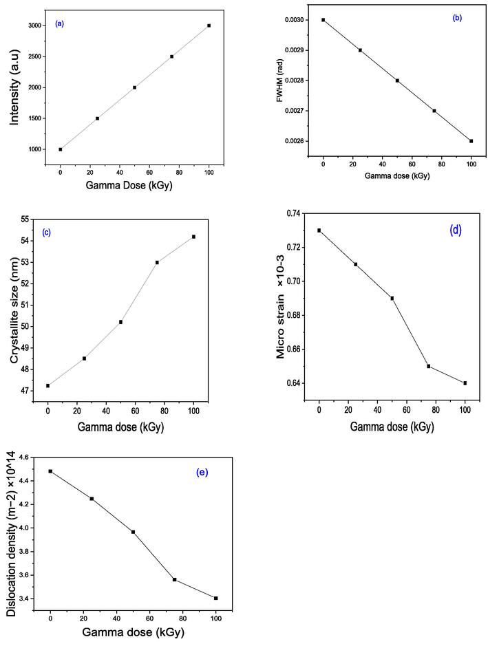
Structural parameter variations of CsPbBr3 thin films: (a) XRD peak intensity, (b) FWHM, (c) Crystallite size, (d) Microstrain, (e) Dislocation density with different gamma dose.
The crystallinity increased as the gamma exposure increased. The crystallite size for pristine and gamma-irradiated CsPbBr3 was measured using the full width at half maxima (FWHM) of the XRD and Scherrer’s formula (Ferrer et al., 2007). Fig. 2-b and 2-c show that the crystallite size increased exponentially, and the FWHM decreased as the gamma dosage increased (Mansoor Ali et al., 2015; Ali, 2019). It can be observed from Fig. 2-d and 2-e that δ and ε decreased as the gamma dosage increased, showing decrease in the lattice imperfections and structural defects caused by gamma irradiation (Mahmoud et al., 2015). The calculated parameters of the XRD results are listed in Table 1.
Sample
Crystallite size D (nm)
Microstrain (ε) × 10−3
Dislocation density (δ) (m−2) × 1014
Lattice parameter
a
(Ǻ)b
(Ǻ)c
(Ǻ)
As deposited
47.240
0.73
4.481
8.326
12.845
8.288
25 kGy
48.516
0.71
4.249
8.331
12.842
8.286
50 kGy
50.214
0.69
3.966
8.329
12.851
8.291
75 kGy
52.992
0.65
3.561
8.331
12.847
8.288
100 kGy
54.192
0.64
3.405
8.328
12.843
8.287
3.2 Surface morphology
The surface morphology of the as-deposited and gamma irradiated CsPbBr3 thin films was investigated using FESEM. Fig. 3(a-e) show that the as-deposited FESEM imagery have small closely packed granular-shaped particles dispersed completely on the surface of substrate. The average grain size decreased as the dosage increased from 0 to 50 kGy and then increased as the dosage increased from 75 kGy to 100 kGy. In our case, the change in grain size has happened due to the defects or radicals created in the molecule after irradiation, and the density of the defects may not be exactly depending on the dosage. It can be also noticed that the small grains are agglomerated, which may be due to the generated heat on the surface of thin films by the incident gamma rays. This indicates that a huge amount of energy was transferred to the structure within a short interval of time. The surface of the thin films appeared irregular and agglomerated in association with the change in the kinetic energy that produced a heating effect, generated by irradiation on the thin film surface (Abhirami et al., 2013). In Fig. 3-f, the energy-dispersive X-ray (EDX) spectrum of the thin film confirms the presence of Cs, Pb, and Br3 in the prepared film and the results exhibit an elemental composition that contains a thin film of superb purity and quality.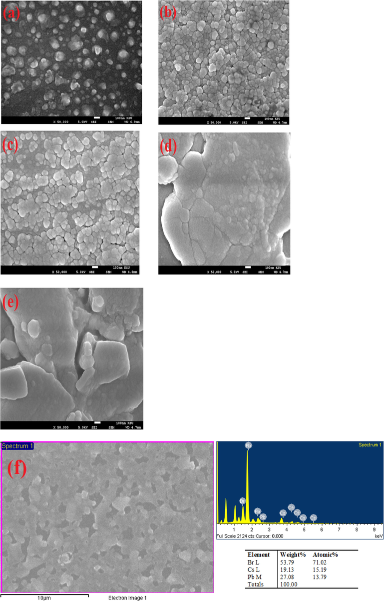
FESEM images: (a) as deposited, b) 25 kGy gamma irradiation exposure, c) 50 kGy exposure, d) 75 kGy exposure, e) 100 kGy exposure, f) EDX spectrum of CsPbBr3 thin films.
3.3 Optical properties
The variations in the band gap of the CsPbBr3 thin films, presented in the Tauc plots (αhν2 Vs hν), are displayed in the inset of Fig. 4. The energy band gap of the pristine thin film was greater than all irradiated samples, where the value of the energy band gap decreased from 2.35 eV to 2.14 eV as the gamma dosage increased from 0 kGy to 100 kGy. This was due to increasing crystallite size and induced defects, due to the gamma exposure having formed localized traps in the energy band gap; matching results were reported by Wahab et al. (Belgacem and Bennaceur, 1990; Wahab et al., 2013). When the wavelength increased from 0 to 50 kGy, a red shift was shown before decreasing from 75 to 100 kGy, when a blue shift was shown. This kind of behavior in the excitonic band is commonly responsible for the characteristics of quantum confinement effects (Abhirami et al., 2013). The electrical conductivity of the thin film improved with the reduction in the band gap after the gamma irradiation interaction, which was closely associated with the transfer of energy that might be the transfer of hole from the valance band to the conduction band with the enrichment of free electrons and holes (Abhirami et al., 2013).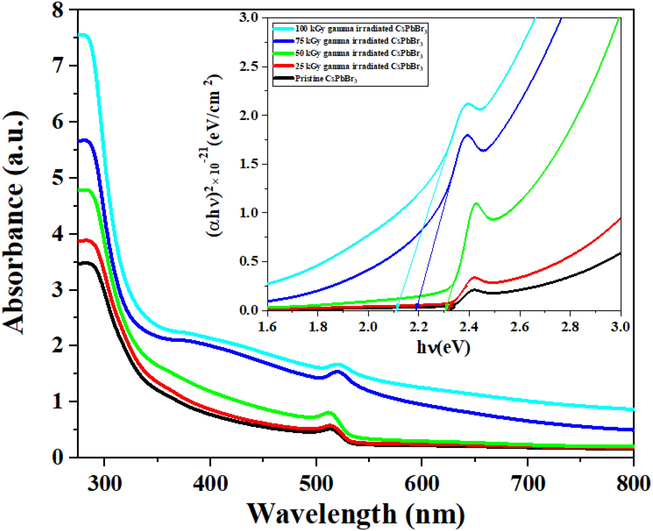
Absorption spectra and Tauc plot of CsPbBr3 with various gamma exposures.
3.4 PL study
The PL spectra used to examine the defect creation/annihilation caused gamma irradiation was recorded at room temperature. The investigation of PL provides confirmation about the defect centers that act as charge carrier recombination centers (Ali, 2020). The PL spectra analysis of CsPbBr3 thin films with different gamma dosages is illustrated in Fig. 5, which shows an excitation wavelength of 500 nm. The measured main transition peak at 517.34 nm was associated with the conduction of valance band transition for all samples. In addition, the enhanced PL intensities as increasing gamma dose from 0 to 100 kGy was attributed to emission spectral broadening and an enhanced recombination rate of electron-hole pairs (Kanemitsu et al., 2002). These effects occurred due to the increased crystallite size, as observed in the XRD results, and the contributions of the excitons trapped within the band gap. The PL peak at 517 nm confirmed the band gap peak, which shifted due to the gamma dosage changes, as already found in absorbance spectra as indicated in Fig. 4.The continuous uptrend of PL peaks to greater wavelengths with increased gamma doses is attributed to a reduction in the energy band gap (Jin et al., 2015). The FWHM of PL illustrated an upward trend with the gamma doses, increasing nonlinearly due to the improvement in the crystallinity and the Frohlich phonons coupling (Liu et al., 2018).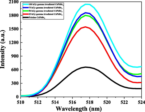
PL spectra of pristine and gamma-irradiated CsPbBr3 thin films.
3.5 Impedance spectroscopy
Electrical impedance spectroscopy is an appropriate technique used to examine the influence of various gamma-dose-induced effects and the internal electoral charge transport process. Fig. 6 demonstrates the Nyquist plots (Z′ against Z″) to reveal the gamma irradiation exposure responses (before and after) on CsPbBr3 thin films at room temperature. The gamma-irradiated thin-film impedance spectroscopy plots exhibit a single semicircle identical to that of an unirradiated thin film (representing the frequency-dependent charge transfer process); in addition, the radius is related to charge transfer resistance. The grain boundary resistance reduced gradually with increasing gamma exposure. The conductivity, as shown in Table 2, increased as irradiation increased from 0 kGy to 50 kGy, decreased at 75 kGy, and increased again at 100 kGy. Different parameters (as dose functions) were calculated by applying the selected fitting equivalent circuit model and are listed in Table 2. On the other hand, in addition to the variation in the electrical parameters after the irradiation is associated with relative to the charge transfer rate. Thus, the less value of the grain resistance is more favorable for improving the charge transport and thus enhancing the sensing behavior of the CuPbBr3 thin films.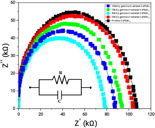
Typical Nyquist plots of as pristine and various gamma-irradiated CsPbBr3 thin films.
Samples
Conductivity
(Ω m)−1 × 10⁻¹⁰
Rg (kΩ)
Cg (pF)
As deposited
8.59
108
8.76
25 kGy
8.67
103
8.35
50 kGy
11.5
78
8.46
75 kGy
9.68
87
8.83
100 kGy
10.45
93
8.64
4 Conclusion
Metal halide CsPbBr3 perovskite thin films were successfully prepared using the thermal evaporation method. They were then comprehensively examined and assessed for different gamma dose effects on their structural, morphological, optical, and electrical properties at dosage strengths of 0 kGy, 25 kGy, 50 kGy, 75 kGy, and 100 kGy. The XRD study indicated that the crystallite size increased, while the dislocation density and microstrain decreased with an increase in gamma dose. FESEM exposed changes in the surface morphology, showing that the grain agglomerated with gamma irradiation due to the high-gamma photon energy transferred to the CsPbBr3 structure. The optical parameters were calculated, the values of which were influenced by the gamma irradiation, the energy band gap decreased from 2.35 to 2.14 eV as the gamma dosage increased. The effect of gamma irradiation exposure on PL properties was also investigated, showing that the intensity and FWHM of PL peaks increased with increasing gamma doses. The impedance analysis revealed that the grain boundary resistance decreased despite conductivity increasing as the gamma dosage increased. These exceptional findings suggest that the CsPbBr3 thin films with different gamma irradiations can be used as superior candidates for sensing materials.
Acknowledgements
The authors would like to extend their sincere appreciation to the Researcher supporting program at King Saud University, Riyadh, for funding this work under the project number (RSP-2021/328).
Declaration of Competing Interest
The authors declare that they have no known competing financial interests or personal relationships that could have appeared to influence the work reported in this paper.
References
- Structural, optical and electrical properties of gamma irradiated SnO thin films. Radiat. Phys. Chem.. 2013;91:35-39.
- [Google Scholar]
- Effect of SHI irradiation on the morphology of SnO2 thin film prepared by reactive thermal evaporation. Vacuum. 2013;90:39-43.
- [Google Scholar]
- A review on organic–inorganic halide perovskite photodetectors: device engineering and fundamental physics. Adv. Mater.. 2017;29(41):1605242.
- [Google Scholar]
- Gamma induced effects on structural, optical and electrical properties of n-TiO 2/p-Si heterojunction. J. Mater. Sci.: Mater. Electron.. 2017;28(21):16314-16320.
- [Google Scholar]
- Gamma irradiation dose dependent nano-structural, optical and impedance spectroscopy of PdS thin films. J. Mater. Sci.: Mater. Electron.. 2019;30(18):17288-17294.
- [Google Scholar]
- Gamma dose dependent structural, optical and current-voltage characteristics of CdS/p-Si heterojunction. Mater. Chem. Phys.. 2020;240:122243
- [Google Scholar]
- Influence of γ radiation on thin Ta2O5–Si structures. Microelectron. J.. 2001;32(7):553-562.
- [Google Scholar]
- Propriétés optiques des couches minces de SnO2 et CuInS2 airless spray. Revue de Physique Appliquée. 1990;25(12):1245-1258.
- [Google Scholar]
- TiO2 nanoparticles arrays ultraviolet-a detector with au Schottky contact. IEEE Photonics Technol. Lett.. 2014;26(11):1065-1068.
- [Google Scholar]
- CsSnI3: semiconductor or metal? High electrical conductivity and strong near-infrared photoluminescence from a single material. High hole mobility and phase-transitions. J. Am. Chem. Soc.. 2012;134(20):8579-8587.
- [Google Scholar]
- An investigation on palladium sulphide (PdS) thin films as a photovoltaic material. Thin Solid Films. 2007;515(15):5783-5786.
- [Google Scholar]
- Anion substitution effects on the structural, electronic, and optical properties of inorganic CsPb(I1–xBrx)3 and CsPb(Br1–xClx)3 perovskites: theoretical and experimental approaches. J. Phys. Chem. C. 2021;125(1):886-897.
- [Google Scholar]
- Gamma irradiation-induced changes at the electrical characteristics of organic-based Schottky structures. J. Phys. D Appl. Phys.. 2008;41(13):135103.
- [CrossRef] [Google Scholar]
- Thallium lead iodide (TlPbI3) single crystal inorganic perovskite: Electrical and optical characterization for gamma radiation detection. Mater. Sci. Semicond. Process.. 2021;121:105392
- [Google Scholar]
- High spectral resolution of gamma-rays at room temperature by perovskite CsPbBr 3 single crystals. Nat. Commun.. 2018;9(1):1-8.
- [Google Scholar]
- Ivanov, L.I., Platov, Y.M., 2004. Radiation physics of metals and its applications. Cambridge Int Science Publishing.
- Structure and photoluminescence of the TiO 2 films grown by atomic layer deposition using tetrakis-dimethylamino titanium and ozone. Nanoscale Res. Lett.. 2015;10(1)
- [CrossRef] [Google Scholar]
- Photoluminescence spectrum of highly excited single CdS nanocrystals studied by a scanning near-field optical microscope. Appl. Phys. Lett.. 2002;81(1):141-143.
- [Google Scholar]
- All-inorganic lead halide perovskite nanohexagons for high performance air-stable lithium batteries. Nanoscale. 2019;11(3):882-889.
- [Google Scholar]
- Organometallic hybrid perovskites for humidity and gas sensing applications. In: 2D Nanomaterials for Energy Applications. Elsevier; 2020. p. :131-147.
- [CrossRef] [Google Scholar]
- Advances in metal halide perovskite nanocrystals: Synthetic strategies, growth mechanisms, and optoelectronic applications. Mater. Today. 2020;32:204-221.
- [Google Scholar]
- Temperature-dependent photoluminescence spectra and decay dynamics of MAPbBr 3 and MAPbI3 thin films. AIP Adv.. 2018;8(9):095108.
- [CrossRef] [Google Scholar]
- Structural, optical and magnetic properties of γ-irradiated SiO2 xerogel doped Fe2O3. Spectrochim. Acta Part A Mol. Biomol. Spectrosc.. 2015;150:72-82.
- [Google Scholar]
- Structural and optical properties of pure and Ag doped ZnO thin films obtained by sol gel spin coating technique. Mater. Sci.-Poland. 2015;33(3):601-605.
- [Google Scholar]
- Progress in the development of semiconducting metal oxide gas sensors: a review. Meas. Sci. Technol.. 2017;28(8):082001.
- [CrossRef] [Google Scholar]
- Nair, G.B., S.J. Dhoble, The Fundamentals and Applications of Light-Emitting Diodes: The Revolution in the Lighting Industry. 2020: Woodhead Publishing.
- 60Co γ-irradiation effects on electrical properties of a rectifying diode based on a novel macrocyclic Zn octaamide complex. Nucl. Instrum. Methods Phys. Res., Sect. A. 2010;612(2):360-366.
- [Google Scholar]
- Fabrication of organometallic halide perovskite electrochemical supercapacitors utilizing quasi-solid-state electrolytes for energy storage devices. Electrochim. Acta. 2020;332:135536
- [Google Scholar]
- A comprehensive theoretical study of halide perovskites ABX3. Org. Electron.. 2016;37:61-73.
- [Google Scholar]
- Perovskites-based solar cells: A review of recent progress, materials and processing methods. Materials. 2018;11(5):729.
- [Google Scholar]
- Thin film organic photodetectors for indirect X-ray detection demonstrating low dose rate sensitivity at low voltage operation. J. Appl. Phys.. 2017;122(22):225502.
- [CrossRef] [Google Scholar]
- 60 Co gamma irradiation effects on the the capacitance and conductance characteristics of Au/PMI/n-Si Schottky diodes. Indian J. Phys.. 2015;89(8):803-810.
- [Google Scholar]
- The long-wavelength edge of photographic sensitivity and of the electronic absorption of solids. Phys. Rev.. 1953;92(5) 1324–1324
- [Google Scholar]
- Optical, structural and morphological studies of (ZnO) nano-rod thin films for biosensor applications using sol gel technique. Results Phys.. 2013;3:46-51.
- [Google Scholar]
- Halide lead perovskites for ionizing radiation detection. Nat. Commun.. 2019;10(1):1-12.
- [Google Scholar]
- A power pack based on organometallic perovskite solar cell and supercapacitor. ACS Nano. 2015;9(2):1782-1787.
- [Google Scholar]
- Nanofiber organic semiconductors: The effects of nanosize on the electrical charge transport and optical properties of bulk polyanilines. J. Appl. Polym. Sci.. 2009;114(2):794-799.
- [Google Scholar]
- Low-dimensional metal halide perovskites and related optoelectronic applications. InfoMat. 2020;2(2):341-378.
- [Google Scholar]