

Translate this page into:
Facile Growth, Physical Characterization, and Dielectric Response of As-Grown NiO Nanostructures
-
Received: ,
Accepted: ,
This article was originally published by Elsevier and was migrated to Scientific Scholar after the change of Publisher.
Peer review under responsibility of King Saud University.
Abstract
FESEM, HRTEM, SAED and rietveld analysis confirmed the nanocrystal structure. NiO in nano-sizes exhibited the high value of optical band gap. Enhanced dielectric properties show the good functional characteristics.
Abstract
Nickel Oxide (NiO) nanostructures were prepared via the hydrothermal technique to examine the structure, optical, and dielectric properties. Various structural, and optical parameters: such as crystal structure, lattice parameter, average crystallite size, average micro-strain, peaks of stretching vibrations, and optical band gap, have been evaluated. Furthermore, the as-prepared NiO nanostructures were used as a dielectric material in a capacitor. Comparatively, the obtained high values of dielectric constant, and low values of dielectric loss show the potential applications of NiO nanostructures as a dielectric material. A possible mechanism has also been illustrated to explain the dielectric behaviour of the as-grown nanostructures.
Keywords
Nanostructures
Rietveld analysis
Optical study
Dielectric properties

1 Introduction
In general, materials with nano-dimension exhibit superior properties compared to their bulk counterparts and that is why nanomaterials are of great importance in nanotechnology. The properties of nanomaterials depend on their dimensions, morphology, shape, crystallinity, etc. Among nanomaterials, semiconducting metal oxides nanostructures are exotic materials due to their functional characteristics and potential applications in electronic and optoelectronic devices (Fischer et al., 2007). Nickel Oxide (NiO) is one of the smart p-type electrochromic semiconductor metal oxide nanomaterial (Ezema et al., 2008). Among the various phases of nickel oxide, NiO is the most stable oxide and has been found in two forms: face-centered cubic (a = 4.1769 Å) (JCPDS: 04-0835) and rhombohedral (a = b = 2.9552 Å, c = 7.2275) (JCPDS: 44-1159). NiO shows good optical, electrical and magnetic properties (Lou et al., 2010; Makhlouf et al., 1997), therefore, it is widely used in sensors (Luyo et al., 2009), transparent electrodes (Marcia-Fantini and Annette Gorenstein, 1987), electronic information display (Yu et al., 1987), electrochromic layers (Ottaviano et al., 2004), dye-sensitized solar cells (Boscholo et al., 2000), and super-paramagnetic materials (Bahari et al., 2008).
Various methods are available for the synthesis of nanostructures such as hydrothermal, sol-gel (Liu and Anderson, 1996), anodic arc plasma (Hongxia et al., 2009), surfactant-mediated (Wang et al., 2002), thermal decomposition (Xiang et al., 2002), polymer-matrix assisted (Deki et al., 2003), and spray pyrolysis (Liu et al., 2003). We have used the facile hydrothermal method to prepare the NiO nanomaterial. The significant advantages of the hydrothermal method over other methods are its simple procedure of preparation in the presence of distilled water, high chemical homogeneity, low processing temperature, stoichiometry control, high purity of the products, low cost, and environmentally benign nature. This method has several other advantages such as rapid diffusion, rapid growth rate, comparatively less synthesis reaction time. It can also produce nanomaterials of high vapor pressure with minimum loss of material. Moreover, the properties, morphology, size, and structure of nanomaterials can be tailored easily by altering the reaction parameters such as reaction time, temperature, reaction medium, pressure, pH, and the concentration of the reactants. (Rangel et al., 2015; Chen, 1998; Bolla et al., 2017).
The electrical properties of capacitors are functions of dielectric behaviour. Dielectric properties reveal the dynamics of a complex inhomogeneous system (Puzenko et al., 2007). Electrical properties of a dielectric material such as polarization, conduction, hopping motion, type of relaxation, etc., can be assessed by exploring the dielectric properties like dielectric permittivity, impedance spectroscopy, electric modulus, etc., of the nanomaterials in a wide frequency range. In general, impedance and modulus spectroscopy reveals the mechanism of conduction, polarization, and relaxation behavior of the dielectric materials (Sharma et al., 2016). Materials of high dielectric constant, show the significant application in capacitors, memory devices, and high K-gate dielectrics (Yu-Jen Hsiao et al., 2007). The dielectric properties of NiO nanostructures were evaluated by ac impedance spectroscopy. This method can reveal the dielectric phenomenon of the material arising inside the electro-active regions due to input ac signal and can explain the mechanism of the obtained dielectric behavior. A functional optical and electrical properties of NiO thin film (Venter and Botha, 2011) indicates the potential application of NiO nanostructures as a dielectric material. The optical and dielectric properties of the materials were found unique when doped with NiO nanostructures. In recent years, NiO nanoparticles based nanocomposites have been extensively exploited as a dielectric material. This is due to their unique dielectric and electro-optical properties for technological, industrial, medical, novel display, and non-display applications. Therefore, it is significantly important to explore the dielectric properties of pure NiO nanostructure (Gaurav et al., 2015). The present paper reports the growth, structural, optical properties of NiO nanoparticles, and a study of its dielectric behaviour as a function of frequency.
2 Material and methods
Nickel Oxide (NiO) nanostructures were prepared by the hydrothermal method. 0.1 M NiCl2 was thoroughly mixed with 100 ml distilled H2O by continuous stirring. During stirring, few drops of NH4OH were incorporated into the solution to maintain the pH value at 10.5. The role of pH (Abdullah, 2017) is to make the solution alkaline for the production of hydroxide ion in large quantity. These hydroxide ions easily replace the chloride ions of the precursor and form the intermediate hydroxide moiety. Which at ambient temperature form desired metal oxide. After that, the prepared solution was heated in an autoclave to 150 °C for 17 hours to carry out the required reaction. As-prepared materials were first washed with acetone. And then dried. Furthermore, all the possible impurities were removed by calcination (at 400 °C for 4 hours).
X’pert PRO (Model: PW 3040/60 of PANalytical) powder x-ray diffractometer (PXRD) was used to examine the crystal structure of as-grown NiO nanostructures. The diffraction pattern was collected using 0.02° step-scan mode at a counting time of 5 seconds. Rietveld refinement was done using the Highscore Plus software, to investigate the nano-crystalline phase and to quantify its structural parameters. Furthermore, the morphological, elemental, structural, optical, spectroscopic, and dielectric analysis was done using field emission scanning electron microscope (FESEM, JSM-7600F, JEOL, Japan), energy dispersive spectroscopy (EDS), high-resolution transmission electron microscope (HRTEM), ultraviolet-visible (UV–VIS) spectrophotometer, Fourier transforms infrared (FT-IR) spectrometer, and LCR meter (MCP BR2827, and 4285A of Agilent) respectively.
3 Results and discussion
3.1 Physical characterization
3.1.1 Rietveld refinement based on powder X-ray diffraction analysis
The presence of intense and sharp diffraction peaks and the absence of diffraction halo in the recorded XRD pattern (Fig. 1(a)) indicate the presence of crystalline phase only and the lack of any amorphous or crystalline-amorphous phase formation, respectively (Abdullah et al., 2014). The obtained and reported (JCPDS: 04-0835) d-values are almost similar, which confirms the cubic system of unit crystal structures.![(a) Powder X-ray Diffraction pattern along with Rietveld refinement of the as-grown nanostructured NiO. The solid black circles and the red line are the observed (Iobs) and calculated (Ical.) NiO X-ray diffraction patterns respectively, the bottom black line is the difference between them (Iobs-Ical) and the vertical lines (l) indicate the NiO reflection lines, (b-c) low to high magnification FESEM images, (d) corresponding EDS-spectrum (e) Lattice resolved HRTEM image, and (f) the SAED pattern along the [1 1 0] zone axis of as-grown well-crystallized NiO nanostructures.](/content/185/2020/32/1/img/10.1016_j.jksus.2019.09.009-fig1.png)
(a) Powder X-ray Diffraction pattern along with Rietveld refinement of the as-grown nanostructured NiO. The solid black circles and the red line are the observed (Iobs) and calculated (Ical.) NiO X-ray diffraction patterns respectively, the bottom black line is the difference between them (Iobs-Ical) and the vertical lines (l) indicate the NiO reflection lines, (b-c) low to high magnification FESEM images, (d) corresponding EDS-spectrum (e) Lattice resolved HRTEM image, and (f) the SAED pattern along the [1 1 0] zone axis of as-grown well-crystallized NiO nanostructures.
Rietveld refinement (Rietveld, 1969) of the x-ray diffraction pattern is known to be an excellent method to extract the structural parameters. In this method the difference between the observed and the calculated intensities of the diffraction pattern is minimized in order to obtain the weighted residual factor
, the expected residual factor
, the R pattern
as well as the goodness of fit
, where ‘Iobs’ and ‘Icalc’ are the observed and the calculated intensities of the diffraction pattern. ‘wi’ is a weighting factor defined as wi = 1/Iobs at the ith step in the diffraction pattern. ‘N’ is the number of experimental observations, and ‘P’ is the number of refined parameters. (McCusker et al., 1999). A NiO cubic system with space group (Fm-3 m (2 5 5)) was used in the refinement, where Ni and O atoms were assigned to specific positions of (4a)(0,0,0) and (4b)(0.5,05,0.5) respectively. A very good Rietveld fit was obtained as shown in Fig. 1(a). Moreover, the fitting parameters (R values) of the final fit are summarized in Table 1, indicating the validity of the fit. The refined lattice parameter a = 4.1770(2) Å.
S. No
Structural Parameter
Rietveld refined value
1
Crystal system
Cubic
2
Space group
Fm-3 m (2 2 5)
3
Lattice parameter
a = 4.1785(2) Å
4
Cell volume
72.9586(3) Å3
5
Crystallite size
25.66 nm
6
Micro-strain
0.340
7
Ni 1 (0, 0, 0)
(4a)
8
O 1 (0.5, 0.5, 0.5)
(4b)
R – factor
9
Rp
9.07
10
Rwp
13.44
11
Rexp
11.4
12
χ2
1.45
A separate refinement was performed to extract the crystallite size and the micro-strain of NiO nanocrystals. To achieve this, a Si standard material was used to evaluate the instrumental broadening (Van-Berkum, 1994), and then subtract it off. Table 1 summarizes the derived structural parameters obtained from the Rietveld refinement of the NiO pattern. The derived average crystallite size is 25.66 nm. Whereas, the average micro-strain is found to be 0.340.
3.1.2 Morphological, elemental, and structural analysis using FESEM, and HRTEM
The FESEM images (Fig. 1(b–c)) show the general morphologies of the as-grown NiO nanostructures. Large numbers of the sphere like shapes can be seen in the low magnification image (Fig. 1(b)). These spheres like shapes exhibit the agglomerated nanostructures of NiO. The average diameter of these spherical-shaped arrays is around 6 μm. Furthermore, the high-magnification FESEM image (Fig. 1(c)) clearly shows the unbroken network of interconnected nanostructures within the spherical shape. Most of these nanostructures depict the sheet-like structures. Typically, the average thickness of these nanosheets is around 50 nm. The EDS spectrum (Fig. 1(d)) of as-grown NiO nanostructures shows the peaks of nickel and oxygen only, and thus indicates the absence of impurity. The elemental composition of Ni and O are in stoichiometric proportion and is in agreement with previous studies (Dıaz et al., 2017).
Furthermore, the crystal structures of as-grown nanostructures were characterized by HRTEM. Fig. 1(e) shows the lattice resolved HRTEM image of NiO nanocrystal corresponding to (1 1 1) crystal plane with a d-spacing of 0.24 nm. Fig. 1(f) represents the corresponding selected area electron diffraction (SAED) patterns along the [1 1 0] axis. The SAED pattern illustrates the perfect rectangular diffraction spots. Which indicates the single crystalline nature of NiO nanocrystals. Dots in SAED pattern correspond to the (1 1 1), (0 0 2), and (2 2 0) planes.
3.1.3 Optical analysis using UV–VIS spectrophotometer
The optical absorption spectrum (Fig. 2(a)) of the as-grown NiO nanostructures demonstrates the common tendency of optical absorption. Fig. 2(a) shows the lower cut off wavelength around 295 nm. Tauc’s relation (1) (Abdullah et al., 2013) was used to evaluate the optical band gap (Eg)
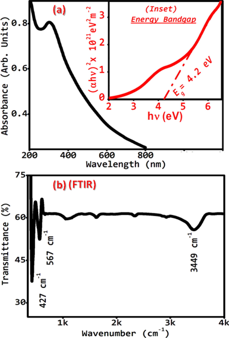
Typical (a) UV–VIS absorbance spectrum, (Inset Fig. 2(a)) direct band gap evaluation, and (b) FT-IR spectra of as-grown NiO nanostructures.
where ‘α’ is the absorption coefficient. ‘A’ is a constant. And ‘n = ½’ for the direct band gap. The direct ‘Eg’ (=4.2 eV) was evaluated by extrapolating the straight line to the energy axis (Inset of Fig. 2(a)). The calculated and reported values (Table 2) are in good agreement (Jian et al., 2012). Earlier reported value of the direct band gap in the corresponding NiO thin film is in the range 2.10 eV − 3.90 eV (Ezema et al, 2008; Marek et al, 2011; Srivastava et al, 2008) whereas, for NiO single crystal it is reported to be equal to 3.87 eV (Dong-Kang et al., 2007). Table 2 shows the highest energy band gap for nanostructures compared to the thin film and single crystal. The variation in energy band gap is due to the possible optical quantum confinement effect. (Abdullah et al., 2015; Zong et al., 2013).
Properties
Single crystal
Thin film
Nanostructures
Eg
3.87
2.1–3.9
4.2
ε
∼11
∼30
42
3.1.4 Spectroscopic analysis using FTIR
The FTIR spectra (Fig. 2(b)) shows the three sharp bands at 427, 567, and 3449 cm−1. The first two bands are attributed to Ni–O stretching-vibration (Dharamraj et al., 2006) whereas, the peak found at 3449 cm−1 corresponds to –OH stretching-vibration (Ikram-ul-Haq, 2010). The band at 3449 cm−1 shows that the specimen has physically absorbed the water molecule during the pellet preparation. The weak serrated peaks in the range 1000–2500 cm−1 demonstrate the presence of O—C⚌O and C—O stretching vibration. This shows that the material absorbed a negligible amount of H2O and CO2 (Hongxia et al., 2009).
3.2 Dielectric properties
3.2.1 Evaluation of dielectric constant (ε)
The response graph (Fig. 3(a) solid blackline) of the frequency dependent dielectric constant (ε) shows that the value of ‘ε’ is lower at higher frequencies. This indicates the presence of all four kinds of dielectric polarization in the low frequency range. Due to this, we found the higher values of ‘ε’ (Abdullah et al., 2011). Simultaneously, Fig. 3(a) (solid blackline) shows a fast decrease in the value of ‘ε’ in the low-frequency region. Such a radical fall is mainly due to the fast decrease in interfacial space charge polarization (Abdullah et al., 2014). Thus, it is found that the space charge polarization is responsible for this dielectric behaviour. The mechanism of the observed trend of ‘ε’ can also be understood more clearly on the basis of a conduction relaxation process, which is related to the charge hopping motion occurring inside the matrix. In the lower frequency region, the randomly oriented motion of the charges generates a higher value of stretching effect inside the matrix. The higher value of the stretching effects amplifies the relaxation time, which in turn increases the hopping length of the charges, and thus produces the higher values of dielectric constant. As the strength of the applied electric field increases with frequency, the electron hoping concentration decreases. Due to this, the value of ‘ε’ in the higher frequency region decreases (Abdullah et al., 2018). The fig (Fig. 3(a) solid blackline) shows that the evaluated values of dielectric constants (9–20) are almost regular in the broad range of frequency (1 MHz − 30 MHz). Therefore, this material can be used in devices to get a steady value of ‘ε’ in this broad frequency range. The value of ‘ε’ for nanostructure was found to increase compared to their bulk counterpart. As, for example, let us consider the frequency of 100 KHz. At this specific frequency, the value of ‘ε’ reported for single crystals and thin films is 11.2 (Rao and Samakula, 1965) and ∼30 (Makhlouf, 2008), respectively while in the present work, it is 42. This distinct higher value of ε is possibly due to the difference in the exposed surface areas of nanosize NiO and bulk size NiO. Furthermore, the dielectric materials of higher values are useful for microelectronic devices such as memory devices, high K-gate dielectrics, etc. (Yu-Jen Hsiao et al., 2007).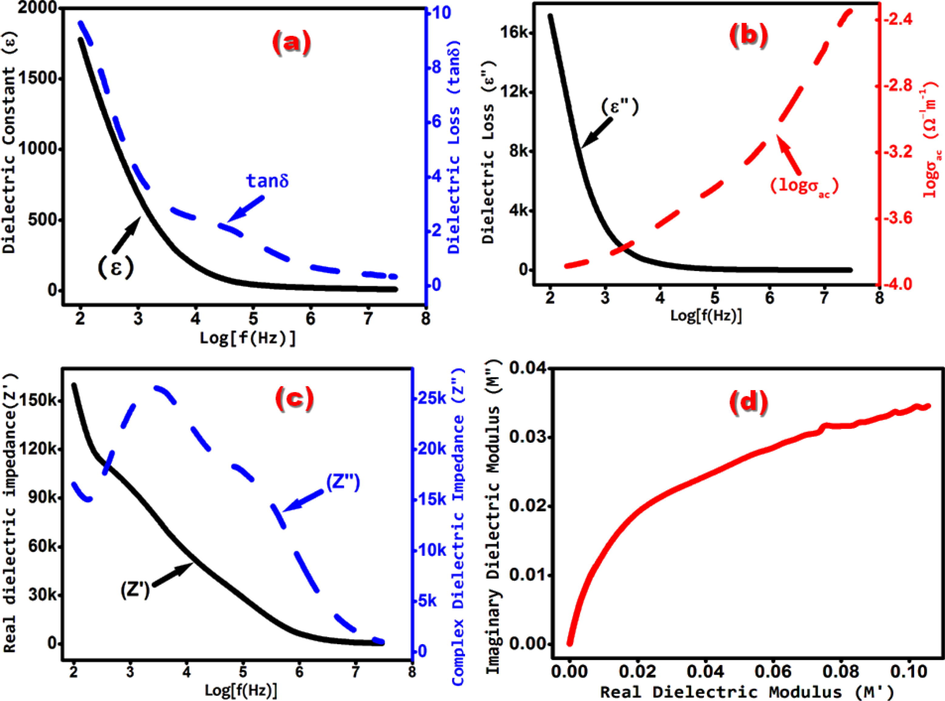
(a) solid blackline shows dielectric constant ‘ε’, and the dashed blueline shows dielectric loss tangent ‘tanδ’ (b) solid blackline shows dielectric loss (ε′′), and the dashed redline shows ac conductivity ‘σac’, (c) solid blackline shows the real dielectric impedance (Z′), and the dashed blueline shows the complex dielectric impedance (Z′′) (d) shows the Cole – Cole plot of real part of the dielectric modulus (M') verses imaginary part of the dielectric modulus (M“) of as-grown NiO nanostructures.
3.2.2 Evaluation of dielectric loss tangent (tanδ), and dielectric loss
The observed behavior of frequency-dependent dielectric loss tangent ‘tanδ’ (Fig. 3(a) dashed blueline) is more or less analogous to the behavior obtained for ‘ε’ (Fig. 3(a) solid blackline). Some small variations are possible due to the relaxation effects occurring because of impurities etc. around the sensitive transition region (Bhatt et al., 2007). On an average, the value of ‘tanδ’ (Fig. 3(b) dashed blueline) is low (9.57–0.32) in the entire frequency region, whereas, it is shallow (0.69–0.32) in the high-frequency range (1 MHz–30 MHz) and is more or less regular. Smaller ‘tanδ’ advocates the enhanced optical quality of the material with minor defects, which is one of the important required parameters for the fabrication of nonlinear optical devices (Abdullah et al., 2011). A strong resistance non-linearity, and third harmonic generation have been explored in NiO thin films (Lee et al., 2008) and giant non-linear absorption in NiO single crystal was also found (Shablaev and Pisarev, 2003). Therefore, the NiO in nano size could be a potential material in non-linear optical devices.
Fig. 3(b) solid blackline, shows the frequency dependence of dielectric loss ( ) for NiO nanostructures. The response graph demonstrates the radical fall in the value of in the low frequency region, whereas it is almost constant and low in the high frequency region. At low frequency, the higher value of is due to space charge polarization, whereas, at the high frequency, lower value of is possibly because of the movement of the free charges. The absence of peaks in (Fig. 3(b) solid blackline) is because of the fact that there is only one straight line in the high frequency region of the graph of ε (Fig. 3(a) solid blackline), which revealed the occurrence of hopping transport mechanism and confirms the non-Deby type dielectric relaxation. (Gaurav et al., 2015; Sharma et al., 2016; Gerhardt, 1994).
3.2.3 Analysis of electrical conductivity
Dashed redline in Fig. 3, shows the characteristic graph of ‘σac’. The graph was drawn using Eq. (2) (Vasudevan et al., 2011)
The figure (dashed redline in Fig. 3) shows almost the frequency independent conductivity in the low-frequency region. Whereas, in the mid and high-frequency range, it shows dependent conductivity. A possible consistent response of conductivity in the low-frequency range corresponds to the dc conductivity. While a relative increase of conductivity in the remaining higher frequency range follows the frequency power law (Jonscher, 1977) as given beow in eq. (4)
This shows that dc conductivity occurs for n → 0, and for ω → 0 limits. Thus we found that the slope of the plotted graph tends to zero in case of dc conductivity. The occurrence of the dc conductivity is because of the loss factor, which has been explained by Jonscher as (Jonscher, 1977)
The mechanism of polarization can be explained in terms of discontinuous hopping of electrons or ions, or jumping of dipoles (Jonscher, 1977). As per jump relaxation model (JRM) (Funke, 1993), the successful hop of charges occurs in the low-frequency range. Whereas unsuccessful hops of ions are attributed to the mid and high-frequency range. The successful hop contributes the long-range translational motion of charges. Which is responsible for the leakage of dc current. The unsuccessful hop of ions contributes the short-range translation movement of ions. The occurrence of unsuccessful hop increases with frequency, which in turn produces the localized or reorientation hopping in the high-frequency region. Thus, it has been found that the successful jump of ions is responsible for the dc conductivity and the unsuccessful hopping is accountable for the ac current.
3.2.4 Impedance and modulus spectroscopy
The solid blackline in Fig. 3(c) shows the variation of real dielectric impedance (Z') with frequency. From the figure, one can find that the values of Z’ decrease as the frequency increase and reached to minimum constant values at higher-frequencies. This tendency of the graph is due to the increase in ac conductivity (σac) with increasing frequency which further confirms the inverse proportional between them. The response graph of Z' in the low-frequency range is accredited to space charge polarization. In the high-frequency range, nearly a shallow constant value of Z′ is due to the inefficient space charge polarization against high-frequency fields. (Jethva and Joshi, 2018; Plocharski et al., 1988; Ganguly et al., 2011).
The dashed blueline in Fig. 3(c) shows the variation of complex dielectric impedance (Z′′) with frequency. From the figure, it has been found that the variation of Z′′ with frequencies exhibit a peak in the low frequency range, and then after that, the value of Z′′ decreases monotonically with increasing frequency in the mid and high frequency region. The appearance of the peak in the low-frequency region indicates the grain boundary relaxation mechanism in the sample (Jethva and Joshi, 2018). The presence of only one peak specifies the presence of a single dielectric relaxation process (Belal and Akhter, 2015). The full-width at half-maximum (FWHM) of a peak reveals the type of relaxation occurring within the dielectric material. For Debye type dielectric relaxation, FWHM of the peak should be less than 1.14 decades (Jethva and Joshi, 2018). But, the calculated value of FWHM of the peak (dashed blueline in Fig. 3(c)) is 1.2 decades, which confirms the presence of non-Debye type relaxation behaviour of the material. The maximum of the peaks (fmax) gives the value of relaxation frequency (Ebru and Ayse, 2012) which is equal to 2000 Hz (dashed blueline in Fig. 3(c)). By knowing the value of ‘fmax’ the value of relaxation-time (τ) can be obtained by using the relation 2πfmaxτ = 1, (Belal and Akhter, 2015) which is found to be equal to 80 microseconds.
The dielectric response of NiO nanoparticles can also be described using the Cole-Cole plot of the real part of the dielectric modulus (M') versus the imaginary part of the dielectric modulus (M“). If the plotted graph represents a semicircle with their center on the x-axis (i.e., on M′′ line), then it indicates a Debye type relaxation in the compound. Otherwise, the curve other than a semicircle confirms the existence of non-Debye type relaxation (Reenu et al., 2015). Fig. 3(d) shows the cole-cole plot of the real (M′) versus imaginary (M′′) part of the dielectric modulus of NiO nanoparticles. The Fig. 3(d) shows a single circular arc in the complex modulus plane. The center of this arc lies below the M′ axis. This confirms the formation of a single phase compound and non-Debye type dielectric relaxation. (Piyush et al., 2012; Shweta et al., 2016).
4 Conclusion
As-grown network of NiO nanostructure shows the enhanced optical, and dielectric properties, and thus reinforces the novelty of the material. Powder XRD, HRTEM, and Rietveld analysis confirm the structural crystallography of as-grown nanostructures. The characteristic peaks of Ni–O stretching-vibration in FTIR spectrum verify the purity of NiO. The higher values of the optical band gap (4.2 eV) and the dielectric constant (e.g., 42 at 105 cps) is attributed to its quantum confinement effect and the large exposed surface area of the nanostructures, respectively. A low value of the dielectric loss shows the good optical quality of the material. The ‘σac’ increases monotonically according to the frequency power law. The Impedance and modulus spectroscopy revealed the non-Debye relaxation behaviour of the dielectric material. A detailed study of dielectric mechanism and their corresponding theoretical interpretation shows the prospective and efficient dielectric features of NiO nanostructures.
Funding
The Author thanks the Deanship of Scientific Research, Najran University, P.O. Box 1988, Najran, 11001, Kingdom of Saudi Arabia, for the financial support of this work under the project Grant Number.: NU/ESCI/15/018.
References
- Structural characterization and frequency dependent dielectric properties of as-prepared Gd2O3 nanorods. Curr. Nanosci.. 2017;13:1-5.
- [Google Scholar]
- Structural and optical characterization of Cr2O3 nanostructures. AIP Adv.. 2014;4:027121
- [Google Scholar]
- Facile growth and promising applications of cobalt oxide (Co3O4) nanoparticles as chemi-sensor and dielectric material. Curr. Nanosci.. 2018;14:1-9.
- [Google Scholar]
- In situ growth and ab initio optical characterizations of amorphous Ga3Se4 thin film: A new chalcogenide compound semiconductor thin film. Scripta Mater.. 2013;69:381-384.
- [Google Scholar]
- Structural and dielectric studies of pure and Mn Doped GaSe. Sci. Adv. Mate.. 2011;3:1-6.
- [Google Scholar]
- Sensitive and fast response ethanol chemical sensor based on as-grown Gd2O3 nanostructures. J. Rare Earth.. 2015;33(2):214-220.
- [Google Scholar]
- NiO nanoparticle synthesis by Chemical Precipitation and effect of applied surfactant on distribution of particle size. J. Nanomat.. 2008;1:1-4.
- [Google Scholar]
- Complex impedance and electric modulus studies of magnetic ceramic Ni0.27Cu0.10Zn0.63Fe2O4. J Adv. Ceram.. 2015;4(3):217-225.
- [Google Scholar]
- Temperature dependence dielectric properties of sodium potassium niobate ceramics. India. J. Pure. Ap. Phy.. 2007;45:609-612.
- [Google Scholar]
- Boscholo, G.B., He, J., Lindquist, S., Hagfeldt, A., (2000). Dye Sensitization of nanostructured NiO. Proceedings of 12th workshop on Quantum Solar energy Conversion-(QUANTSOL 2000), Wolkenstein, Studtirol, Italy.
- Chapter 1 – Novel approaches for preparation of nanoparticles, Book Title: Nanostructures for novel therapy: Synthesis, Characterization and Applications. Book Seies: Micro and Nano Technologies, Elsevier; 2017. p. :1-36.
- Hydrothermal Epitaxy of Peroksite Thin Films. Doctor of Philosophy: University of California; 1998.
- NH2-Terminated Poly (ethylene oxide) Containing Nanosized NiO Particles: Synthesis, Characterization, and Structural Considerations. Chem. Mater.. 2003;15:4916-4922.
- [Google Scholar]
- Synthesis and magnetic properties of nanostructured metallic Co, Mn and Ni oxide materials obtained from solid-state metalmacromolecular complex precursors. RSC Adv.. 2017;7:27729.
- [Google Scholar]
- Optical properties of black NiO and CoO single crystals studied with spectroscopic ellipsometry. J. Korean. Phys. Soc.. 2007;50(3):632-637.
- [Google Scholar]
- Electrical Properties and Impedance Spectroscopy of Pure and Copper-Oxide-Added Potassium Sodium Niobate Ceramics. IEEE. T. Ultraso. Ferr.. 2012;59(10):212-2128.
- [Google Scholar]
- Ac conduction in amorphous chalcogenide and pnictide semiconductors. Adv. Phs.. 1987;36(2):135-217.
- [Google Scholar]
- Optical properties of chemical bath deposited nickel oxide (NiOx) thin films. Superficies y Vacío.. 2008;21(1):6-10.
- [Google Scholar]
- Incorporation of homogeneous, nanoscale MnO2 within ultraporous carbon structures via self-limiting electroless deposition: implications for electrochemical capacitors. Nano Lett.. 2007;7:281.
- [Google Scholar]
- Structural, dielectric and electrical properties of CaBa4SmTi3Nb7O30 ferroelectric ceramic Bull. Mater. Sci.. 2011;34:907.
- [Google Scholar]
- Effect of nickel oxide nanoparticles on dielectric and optical properties of nematic liquid crystal. AIP Conf. Proc.. 2015;1675:030065
- [Google Scholar]
- Impedance and dielectric spectroscopy revisited: distinguishing localized relaxation from long-range conductivity. J. Phys. Chem. Solids.. 1994;55(12):1491-1506.
- [Google Scholar]
- Hongxia Q., Zhiqiang W., Hua Yang, Lin Zhu, Xiaoyan Yan, 2009. Preparation and Characterization of NiO Nanoparticles by Anodic Arc PlasmaMethod. J. Nanomater.-Hindawi Publishing Corporation. Article ID 795928, 1-5.
- Synthesis and Characterization of Uniform Fine Particles of Nickel Compounds. J. Chin. Chem. Soc.. 2010;57:343-347.
- [Google Scholar]
- Impedance, modulus and spectroscopic analysis of gel-grown pure lead levo-tartrate crystals. Bulg. J. Phys.. 2018;45:275-284.
- [Google Scholar]
- Preparation of high aspect ratio nickel oxide nanowire and their gas sensing devices with fast response and high sensitivity. J. Mater. Chem.. 2012;22:8327-8335.
- [Google Scholar]
- Strong resistance nonlinearity and third harmonic generation in the unipolar resistance switching of NiO thin films. Appl. Phys. Lett.. 2008;93:252102
- [Google Scholar]
- Porous nickel oxide/nickel films for electrochemical capacitors. J. Electrochem. Soc.. 1996;143:124-130.
- [Google Scholar]
- Preparation of Nanoscale NiO Powders by Polymer-network Gel Process. Chin. J. Inorg. Chem.. 2003;19:624-626.
- [Google Scholar]
- The influence of annealing on electrochromic properties of Al–B–NiO thin films prepared by sol–gel. J. Sol. Gel. Sci. Technol.. 2010;54:43-48.
- [Google Scholar]
- Gas sensing response of NiO nanoparticle films made by reactive gas deposition. Sensor. Actuat. B-Chem.. 2009;138:14-20.
- [Google Scholar]
- Electrical properties of NiO films obtained by high-temperature oxidation of nickel. Thin Solid Films.. 2008;516:3112-3116.
- [Google Scholar]
- Electrochromic nickel hydroxide films on transparent/conducting substrates. Sol. Energ. Mater.. 1987;16:487-500.
- [Google Scholar]
- Electrical and optical properties of NiO films deposited by magnetron sputtering. Opt. Appl. XL. 2011;I(2):431-440.
- [Google Scholar]
- Electrochromic nickel oxide films made by reactive r. f sputtering from different targets. Surf. Interface. Anal.. 2004;36:1335-1339.
- [Google Scholar]
- Study of Structural and Electrical Properties of a New Type of Complex Tungsten Bronze Electroceramics Li2Pb2Y2W2Ti4V4O30. J. Modern Phys.. 2012;3:870-880.
- [Google Scholar]
- Electrochemical stability and ionic conductivity of some polymerlic based electrolytes. Solid State Ionics. 1988;28–30:979-983.
- [Google Scholar]
- Dielectric behavior and percolation phenomena in porous silica gels. Chem. Phys. Lett.. 2007;324:7-14.
- [Google Scholar]
- Advantages of hydrothermal synthesis to produce tunable TiO2 nano micro sized photocatalysts and their effect in lignin degradation. NANO: Brief Rep. Rev.. 2015;10(3):1550046.
- [Google Scholar]
- Dielectric properties of cobalt oxide, nickel oxide, and their mixed crystals. J. Appl. Phys.. 1965;36:2031-2038.
- [Google Scholar]
- Impedance spectroscopy and dielectric studies of nanocrystalline iron doped barium strontium titanate ceramics. Process. Appl. Ceram.. 2015;9(2):73-79.
- [Google Scholar]
- A profile refinement method for nuclear and magnetic structures. J. Appl. Cryst.. 1969;2:65-71.
- [Google Scholar]
- Giant nonlinear absorption in the NiO antiferromagnet. Phys. Solid. State.. 2003;45(9):1742-1745.
- [Google Scholar]
- Complex dielectric and impedance behavior of magnetoelectric Fe2TiO5. J. Alloys Compd. 2016;663:289-294.
- [Google Scholar]
- Impedance and Modulus Spectroscopy Characterization of Tb modified Bi0.8Tb0.1Pb0.1Fe0.9Ti0.1O3 Ceramics. Mat. Res.. 2016;19(1):1-8.
- [Google Scholar]
- Preparation, Microstructure and Optical Absorption Behaviour of NiO Thin Films. J. Nano. Sci. Nanotechno.. 2008;8:4111-4115.
- [Google Scholar]
- Strain Fields in Crystalline Materials. Dleft University of Technology, The Netherlands; 1994. PhD. Thesis
- Synthesis, growth, optical, mechanical and electrical properties of L-lysine L-lysinium dichloride nitrate (L-LLDN) single crystal. Bull. Mater. Sci.. 2011;34(3):469-475.
- [Google Scholar]
- Optical and electrical properties of NiO for possible dielectric applications. S Afr. J. Sci.. 2011;107(1/2) Art. #268, 6 pages
- [Google Scholar]
- Preparation of nanocrystalline metal oxide powders with the surfactant-mediated method. Inorg. Chem. Commun.. 2002;5:751-755.
- [Google Scholar]
- Experimental study on synthesis of NiO nanoparticles. Scripta Mater.. 2002;47:219-224.
- [Google Scholar]
- Spectroscopic and electrochemical studies of electrochromic hydrated nickel oxide films. Sol. Energ. Mater.. 1987;16:1-17.
- [Google Scholar]
- Yu-Jen Hsiao, Yee-Shin Chang, Te-Hua Fang, Yin-Lai Chai, Chao-Yu Chung; Yen-Hwei Chang, 2007. High dielectric permittivity of Li and Ta codoped NiO ceramics. J. Phys. D: Appl. Phys. 40, 863–868.
- Cu2ZnSnSe4 quantum dots with controllable size and quantum confinement effect. J. Nanopart. Res.. 2013;15:1947-1953.
- [Google Scholar]