

Translate this page into:
Fabrication and characterization of field effect transistor based on single walled carbon nanotubes
⁎Corresponding authors. mzamzami@kau.edu.sa (Mazin A. Zamzami), nate.ahn@gmail.com (Saeyoung Nate Ahn)
-
Received: ,
Accepted: ,
This article was originally published by Elsevier and was migrated to Scientific Scholar after the change of Publisher.
Peer review under responsibility of King Saud University.
Abstract
Objectives
Sensor biology and sensor devices have been advancing since its inceptions. In this work, we report fabrication of carbon nanotubes filed-effect transistor (CNT-FET) sensor and its characterization. CNT intensively has been used in the construction of sensing layers due to their exceptional features, large surface area, stability, high mechanical strength, adaptability, and functional behavior.
Methods
Carbon nanotubes (CNTs) as semiconductor were fabricated as an active nanomaterial between the source-drain electrodes. The fabrication of CNT-FETs performed by following conventional photolithography method and lift-off techniques.
Results
The structural morphology of deposited CNT was confirmed by the scanning electron micrograph (SEM) imaging. The transfer curves between drain-source were considered as a function of the drain-source voltage (VDS) and gate-source voltage (VGS) from individual CNT-FET fabricated wafer. The characterized Ion/Ioff ratio was calculated for every CNT-FET device. The semiconductor properties of the fabricated CNT-FET device characterized by the source-drain current (IDS) versus gate voltage (VGS).
Conclusions
CNT-FET based device have advantages of low cost fabrication, quick response, increased sensitivity, small size, and high flexibility. CNT-FETs have been used comprehensively in the biosensing of chemicals, proteins, nucleic acids, bacteria, and virus etc. This device could be used for SARS-CoV-2 and related variant detection in current scenario.
Keywords
Carbon nanotubes
Field-effect transistor
Scanning electron micrograph
PBASE

1 Introduction
Single walled carbon nanotubes (SWCNTs) are cylindrical and hollow long tube-like structure and diameters ranging from 1 to 100 nm. CNTs are emerging as building blocks for novel nanostructures used in diagnostic devices (Venkataraman et al., 2019). CNTs are hollow cylinders of sp2 bonded carbon atoms and unique among solid state materials in that all atoms are on the surface (Ma et al., 2010). CNTs in functional condition carry a unique combination of excellent electrical, mechanical and electrochemical features (Goh et al., 2014). These incredible features of CNTs attract the interest of the researchers as a principle fabrication nonmaterial of biosensors (Luong et al., 2007). In nanometer scale size, the CNT dimension is close to the size of several molecules of interest, indicating a distinctive biocompatible detection platform (Chen et al., 2014; Menard-Moyon et al., 2010). The novel and useful characteristics of CNTs, such as low-cost, light-weight, distinct optical feature, high surface, high aspect ratio, high mechanical, high thermal, high electrical properties make suitable for the fabrication that allows wide range of biomedical and industrial applications (Anzar et al., 2020; Kim et al., 2018). All these properties good suitable to stimulating electron transfer reactions for many detecting biomolecules (Polizu et al., 2006). CNT can perform the electron transfer without scattering over relatively large distances such as several micrometers depending upon the mechanical property of the nanotubes (Chen et al., 2018). However, the hydrophobic nature of CNT promotes insolubility in polar solvent and this property is not compatible with biomacromolecules solubility nature (Chen and Mitra, 2019). Based on the relying properties of their optical features, it is used as optical tags or contrast agents for collecting biological image for diagnosis of diseases (Zamzami et al., 2022). SWCNTs carry various desirable structure-dependent electronic and mechanical features (Takakura et al., 2019). These features contribute to the possibility of manufacturing stable and superior electrochemical biosensors. After surface modification, CNTs can be allowed to react with thiol group, EDC/NHS and PBASE. CNTs containing functional groups have increased interaction with target biomolecules on the inorganic/organic matrices via van der Waals interaction covalent or hydrogen boding depends on the type of surface modifying agents (Liu et al., 2009). After surface modification, the CNT possess significant potential biosensors due to their ease in immobilized target antibody and maintains the proteins inherent property (Yüce and Kurt, 2017).
The CNT field effect transistor (CNT-FET) based on SWCNTs includes high intrinsic sensitivity, well-known carbon surface chemistry that enables versatile methods of functionalization, and antibody immobilization has been successfully pursued in the past (Byon and Choi, 2006). In 1998 first CNT-FET was fabricated and developed by Dekker's group (Tans et al., 1998), later researcher have working on the optimization of materials and improved performance of the device. The transistor operates under one gate and two carrier source-drain field induced modulation of the band structure at the contacts (Appenzeller et al., 2002). CNT-FET devices have been widely used as all electronic transduction components in both highly specific biosensors based on antibody-antigen type interactions. The main merits of the CNT-FET based sensor is easy fabrication steps, quick sensing response, ease of handle, because accurate dynamic real time sensing response are imperative for disease diagnosis, food safety and environmental monitoring (Liu and Guo, 2012; Liang et al., 2020; Hosseingholipourasl et al., 2020).
In this study, we demonstrate the fabrication and characterization of CNT-FET devices. CNT-FET was fabricated through conventional photolithography method and drop coating CNT between two electrodes Au/Ti on the silicon dioxide/silicon substrate. The fabricated CNT-FET device has more stability against chemical treatment and passivated with SU-8 to prevent the short circuit of the electrodes. The device has more stable current showing that fabricated CNT material strongly attached with the substrate surface. In this fabrication non-metallic CNT material was used to improve the semiconductor properties of the CNT-FET devices. The gate current leakage is negligible (between 1 and 2 nA range) which proves that CNT-FET devices well fabricated. The microstructure and morphology of the deposited CNT was characterized by SEM imaging. The surface of CNT non-covalently functionalized with PBASE. XPS was used to characterize the change in surface modification of CNT after bifunctional molecule, 1-pyrenebutanoic acid N-hydroxysuccinimide ester (PBASE) dissolved in 1,2-dicholorobenzene (o-DCB). The schematic fabrication diagram of the FET device is shown in Fig. 1.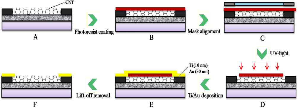
Photograph of wafer scale fabricated CNT-FET devices and electrode patterning. Step (A) Deposited CNTs on the Si/SiO2 surface, step (B) Photoresisit coating, step (C) mask alignment, step (D) UV-light treatment, step (E) Ti/Au deposition and step (F) lift-off removal.
2 Materials and sample preparation
2.1 Materials source
Single walled carbon nanotubes (SWCNTs) were purchased from the Nano Integris, Canada, whose diameter and length were 1–2 nm and 5–30 µm respectively. The linker molecule 1-pyrenebutanoic acid N-hydroxysuccinimide ester (PBASE, Cat# 457078) and 1,2-dicholorobenzene (o-DCB) 99% purity grade were received from Sigma Aldrich. A 350 µm thick n-type 〈1 0 0〉 silicon (Si) wafer and 4-inch diameter was purchased from Waferbiz, Korea. All the buffer solutions were prepared in deionized (DI) water resistivity of 18.2 MΩ/cm. The pure DI water was collected from an MDM Wellix Plus water purification system (MDM Corporation, South Korea). All other chemicals used in this research were of high purity analytical grade and used as received from commercial sources without further purification.
2.2 Dispersion of CNTs and suspension preparation
CNTs have the agglomeration tendency, for uniform dispersion is big issue and its applications in industry. The ultrasonic dispersion method is considered an effective, less time taking compared to the conventional dispersing methods. However, long duration sonication or high energy used in solubilization can damage the structure and other properties of the CNTs (Daneshvar et al., 2021). A suitable combination of mechanical and chemical stress can reduce the structure damage and integrity of the suspended CNTs in the solvent. SWCNT bucky paper 0.001, 0.01 and 0.1 mg/mL dispersed in 1,2-dichlorobenzene (o-DCB) solvent and followed ultrasonication procedure for 10 min to achieve the homogeneous CNT suspension and there are no bundled particles confirmed by naked eye. The CNT suspension in o-DCB followed by 20 min centrifugation at 10,000 rpm and supernatants of tubes were collected after centrifugation. Fully dispersed CNT solutions were transferred into new storage vial. CNT suspension filtered through the 0.2 µm PVDF Whatman syringe type filter into fresh vial and final volume were brought up to 1.0 mL with o-DCB. After filtration of CNT pooled suspension were again sonicated for 2 min to dissolve any un-dissolved species. The filtered CNT suspension loaded in cartridge of inkjet printer and uniform CNT layer generated by inkjet nozzle. To fix the CNT on the SiO2 surface printed chips were annealed at 120 °C in vacuum oven for 24 h.
2.3 Preparation of 1-pyrenebutanoic acid N-hydroxysuccinimide ester (PBASE) suspension
The linker solution was prepared by dissolving 7.7 mg PBASE powder in 10 mL methyl alcohol and gently agitated for mixing 1 h in ambient and dark room to achieve absolute mixing of PBASE powder. The PBASE suspension solubility was confirmed by the necked-eye and suspension was transparent and clear.
2.4 CNT-FET fabrication and deposition of metallic electrodes
The sensing channel was patterned using conventional photolithography process. The substrate was placed on the spin-coater and positive photoresist was drop-coated at 3000 rpm for 50 s to produce uniform resist coating. The substrate was further placed on the mask aligner under photo mask and exposed to UV light for 15 s. The patterning and generation of metallic electrodes Ti/Au 10/30 nm thick films were deposited using conventional photolithography and typical lift off process. All these fabrication materials were deposited on the 1 µm thick layers of SiO2 functions as dielectric gate. The CNT deposited outside of the channel area were removed by implementing proper patterning process, including a photolithography process using the sequential oxygen gas or plasma treatments for selective etching. The metallic electrode spacing was 10 µm between the sensing areas. Finally, gate dielectric patterning was generated via a negative photoresist-based photolithography process and subsequent lift-off steps. To block the direct connection with source-drain electrode metal surface reduce the loss of electrical signal in IDS measurements, SU-8 photoresist passivation has been carried out to provide shielding.
2.5 Optical and scanning electron microscopic imaging
An optical microscope (Olympus BX53MRF-S) equipped with a 10 × DF objective lens and a camera was used to observe the orientation and alignment of the fabricated CNT-FET device. Microstructure and morphology of the fabricated CNT-FET device were visualized by FE-SEM, JEOL JSM-7610F (JEOL Ltd, Akishima, Japan). The double-sided adhesive carbon tape was stick on the round sample holder and CNT-FET devices were mounted on top of the carbon strips and transferred into the thermovac chamber for removal of existing moisture. The sample holder containing CNT-FET was transferred into the holder knob inside of the SEM machine chamber and captured the image of desired area.
2.6 CNT surface functionalization via PBASE
The suspended PBASE stock solution was diluted in pure methanol and poured in the fresh vial. CNT-FET devices were soaked in vial containing PBASE solution for non-covalent surface modification in dark at room temperature. The best surface modifications were optimized by soaking CNT-FET in increasing molar concentration of PBASE 0.1, 0.4, 0.8, 1.2, 1.6 and 2 mM. After 1 h incubation immersed CNT-FET devices were removed from the vial containing PBASE solution and rinsed three times with pure methanol to remove unbound or un-reacted PBASE molecules from the CNT surface and N2 gas blow was used for dry purpose. The PBASE modified surface maximizes the device performance and sensitivity of CNT-FET devices. The PBASE modified dried CNT-FET devices were characterized by XPS measurements and compared with bare CNT-FET surface.
2.7 XPS measurements
X-ray photoelectron spectroscopy (XPS) data were collected on K-Alpha (Thermo Fisher Scientific, USA) spectrometer. The XPS machine is attached to a monochromatic AlKα X-ray source (1486.6 eV). The XPS emission source were run at 10 mA current at 12 kV (120 W) anode potential. The ejected photoelectrons were accumulated with the precision high energy electron analyzer mode with the constant pass energy of 200 eV. During sample scan the energy resolution of the analyzer were consistent throughout experiment. For consistent digital fitting and compositional analysis, Thermo Scientific Advantage software package was used as supplied by the manufacturer.
2.8 I-V measurements
For the characterization of the fabricated CNT-FET semiconductor electrical properties of the device measurements were carried on the Keithley 3 probe station at ambient condition. The transfer properties of deposited CNTs, the current between the source and drain (IDS) was measured by applying (VGS) −1.5 to 0.5 V to the back gate that facing the opposite side of the CNTs.
3 Result and discussion
3.1 Wafer-scaled CNT-FET device fabrication and characterization
The thickness of silicon (Si) wafer was 350 µm, 4-inch diameter and carries a resistance of 3 Ω/cm. Initially cleaned and dried Si wafer loaded into the quartz wafer holder in a diffusion furnace chamber. The diffusion furnace chamber can operated either wet oxidation or dry film growth by controlling the turn knob. High purity oxygen gas flushed into the quartz wafer holder and ensures that no air impurities are supplied during the formation of oxide layer. When the wet oxidation procedure introduced water vapors into the furnace chamber was typically generated by passage as a carrier gas into a tank filled with ultrapure DI water and temperature was maintained below the boiling temperature (100 °C). The used carrier gases can be either oxygen or nitrogen both gas combination results in equivalent growth rates and oxide thickness layer. The thick layer of 30 nm SiO2 film was sputter-deposited onto the Si wafer and the deposited SiO2 layer works as the insulator and date electrode for the fabricated FETs.
3.2 Source-drain (S-D) electrode fabrication
To grow thin films of titanium (Ti)/gold (Au) electrodes on the substrate as back gate (G). Inkjet printing technique has been used to deposit the CNT network on the substrate material as described in our previous publication (Zamzami et al., 2022). CNT-FETs device fabrication steps including source-drain electrodes are shown in Fig. 1A–F. The primary mask was used to identify and patterning of S-D electrodes with distance of about 3 µm Au, (99.99% pure from Alfa Aesar) using standard ultraviolet (UV) photolithography 5 nm thick Ti/100-nm thick and metal lift-off processes (Fig. 1E and F). To increase the adhesion property of Au at the bottom layer the thin layer of Ti was applied on top of the Au layer. As shown in Fig. 2A, the scalable printing process to produce bulk quantity of CNT-FET devices on wafer scale. CNT also dispersed on the bottom background surface and for removal an extra etching step using O2 plasma was utilized to reduce the possible gate current leakage. The wafer device contains total 84 CNT-FETs (Fig. 2A). The optical microscope (OM) image of wafer shows fabricated CNT-FET chips containing 84 electrode sets, on top of surface CNTs were printed by inkjet printer. Photograph of the wafer after Ti/Au electrode patterning on the wafer (Fig. 2B and C). Pure acetic acid and DI water washing was done for the wafer cleaning for 1 min and wet surface was dried with N2 gas blow. Device characteristics were tested for multiple configurations on the same electrode.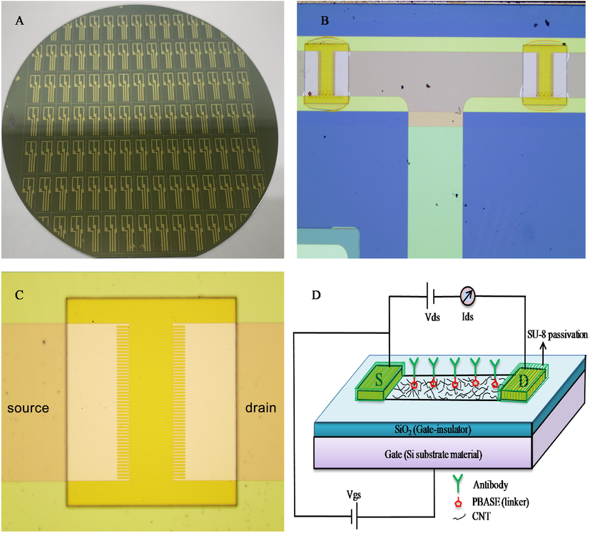
(A) Optical image of the full size wafer (4 inch) and CNT-FET. (B) Optical microscopic image showing the source-drain electrode. (C) Source-drain electrode shown in high magnification scale. (D) Schematic image showing CNT-FET sensor that illustrates the structural components and circuit diagram.
3.3 Characterization of deposited CNT by SEM imaging
The microstructure, size and alignment of CNT at three increasing concentration (0.001, 0.01 and 0.1 mg/mL) of CNT suspension were deposited on the sensing channel of the device and were characterized by FE-SEM imaging. Fig. 3A shows that bare Si/SiO2 surface has no any debris, junk and abnormal color after surface cleaning. Five different locations were selected for visualize the deposition uniformity of the deposited CNTs. Fig. 3B-D shows the surface morphology of concentration dependent CNT deposited between the source-drain electrodes. CNTs at lower concentration was printed between the pair of source-drain electrodes as shown in Fig. 3B very few needle like CNT microstructure observed. It can be seen that with increasing concentration of CNT suspension deposited on the surface, results more CNT flakes were deposited at the targeted area. The visualized SEM in Fig. 3B shows that very less CNT density (0.001 mg/mL) deposited on the Si/SO2 surface. Fig. 3D attributed to the best deposition and homogeneity of the CNT on the surface. It can be seen that deposited CNTs are mostly individual, and they are well distributed on the Si/SO2 surface.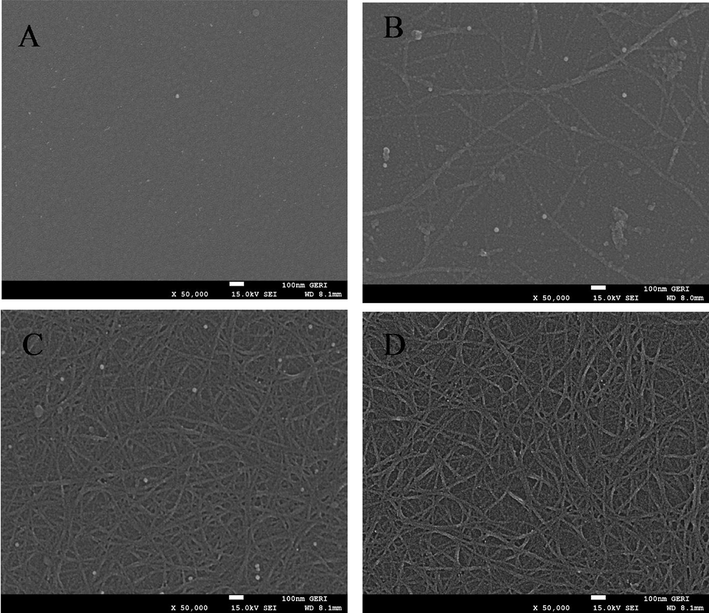
FE-SEM images for surface morphology of different concentration of CNT deposited on the sensing area between the source-drain electrodes. The FE-SEM images showing CNTs deposition correspond to the approximate one best out of five captured locations. The scale bars are selected 100 nm. (A) Bare Si/SO2 surface (B) 0.001 mg/mL (C) 0.01 mg/mL (D) 0.1 mg/mL.
3.4 Dispersion of CNT in o-DCB
CNTs molecules are extremely hydrophobic in nature, poorly soluble in either water or organic solvents and highly aggregation prone in solvents medium, which limits their application (Li and Qiu, 2019). Proper dispersion of CNTs raises a concern in pharmaceutical industry and its applications in accurate concentration determination. (Ivanova et al., 2012). Therefore UV–visible near infrared absorbance can give highest only for maximally exfoliated CNTs (Grossiord et al., 2007). It is high chance that CNTs can be re-agglomerating within a time period in the course of deposition. After agglomerate formation absorbance values of dispersed CNTs continuously decreased and found that reduced number density interferes the precision of device fabrication. Previously it has been documented that the SWCNTs show the highest solubility in organic solvents such as DMF (Boul et al., 1999), NMP (Yau et al., 2015) and o-DCB (Bramhe et al., 2016).
3.5 XPS for CNT-FET surface modification by PBASE
XPS is a surface analytical technique that is useful for the elemental identification and semi-quantification of surface states. The positions of the photoemission peaks can be related directly to the energy of the electron being excited from a core level. Thus, changes in the chemical environment of an element results in changes in the peak position of that element in the XPS spectrum. This change in binding energy is called the chemical shift. The chemical shifts can therefore be used to characterize the surface functionalities of solids. To functionalize the CNT-FET devices we have followed the previously described protocol (Zamzami et al., 2022). Fabricated CNT-FET devices were soaked in PBASE solution and used different molar concentration. The immobilization of PBASE linker to develop antibody modified CNT-FET sensor for antigen detection. An aliquot of PBASE solution increasing molar concentration was used to soak the device and incubated for 1 h at room temperature. Then the device was extensively rinsed with pure methanol. XPS was utilized to determine the surface modification SWCNT. The XPS spectra of the bare SWCNT and PBASE modified surface are shown in Fig. 4. The SWCNT before surface modification their unique structural elements e.g., C and O. The characteristic minor peak carbon (C1s) at 285.3 eV and major peak of oxygen (O1s) were detected before PBASE treatment at 533.1 eV respectively (Fig. 4A). The peak C1s originated due to the C–C bonds sp3 hybridization of the SWCNTs. However, the peak O1s originated due to the O-C bond. As shown in Fig. 4B the C1s peak shifted toward a lower binding energy if CNTs accepted electrons from surroundings and vice versa. The data analysis revealed that PBASE treatment increased the atomic percentage of O1s from 19.3 to 23.2%.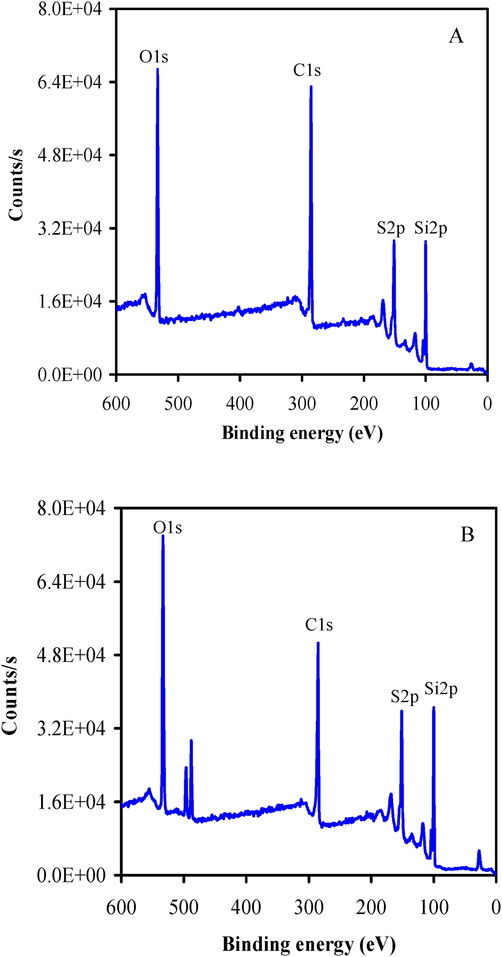
X-ray photoelectron spectroscopy (XPS) spectra of CNT (A) before surface modification (B) after surface modification by PBASE.
3.6 Optimization of PBASE concentration surface modification
The systematic immobilization of PBASE linker was investigated and shown in Fig. 5A. Previously researchers have been reported that the SWCNT-based FETs functionalized with PBASE showed a 5–10% loss in IDS in the ON state. The relative decrease in the ‘ON’ current (ΔI/ΔImax), where ΔImax suggests the decrease in ‘ON’ current at saturation point due to the strong binding of PBASE and CNTs graphite surface. The obtained ΔI/ΔImax continuously increases from PBASE concentration 0.1 to 2 mM and achieved saturation at 2 mM (Fig. 5B). Considering pyrenes molecule is the well-known popular aromatic species for non-covalent attachment with sidewalls of CNT through π–π stacking (Fernando et al., 2004; Liu et al., 2008; Kimura et al., 2009). The π–π stacking between the CNT and PBASE affects the hole carrier flowing bottom side of the CNT channel leading to the observed increase in ΔI/ΔImax(Star et al., 2003). An additional approach has been followed to verify the surface adsorption by PBASE. The surface functionalization determines the formation with sidewall of CNT via directional π–π stacking of the aromatic pyrene molecules (Guadagno et al., 2018). This indicates that the PBASE successfully makes SAM layer on the CNT-FET surface. Therefore 2 mM PBASE concentration was selected for the subsequent experiment.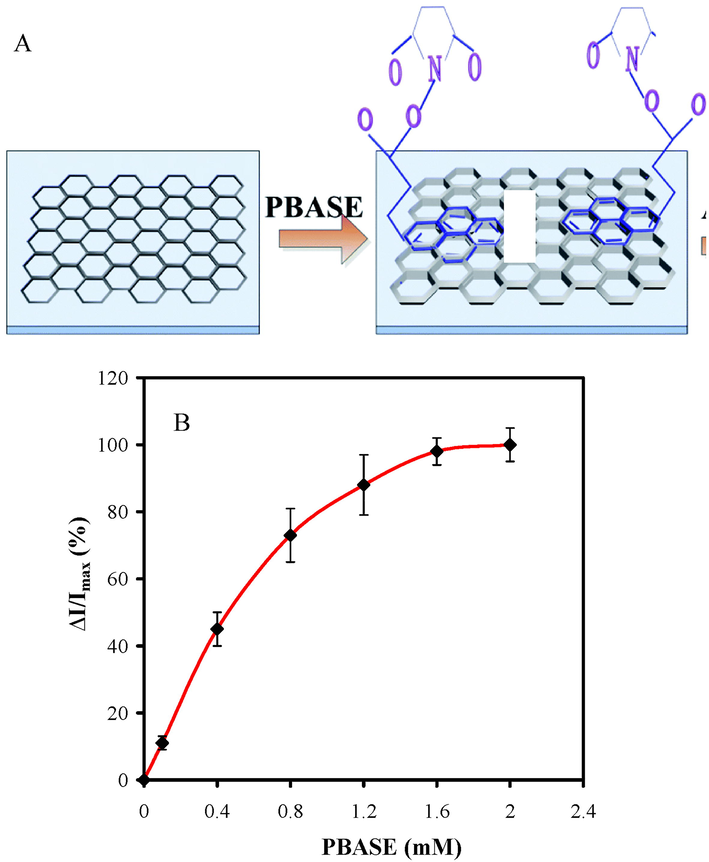
(A) SWCNT surface and anchored PBASE linker (B) PBASE linker concentration optimization on the CNT-FET sensor.
3.7 Transfer characteristics validation of the CNT-FET
Upon sensor fabrication completion, each CNT-FET devices on the Si/SiO2 wafer were connected with three probe station and semiconductor behavior were observed one by one as discussed in method section. After device transfer characteristics measurements it was observed that on the wafer 76 (87%) of the 84 CNT-FETs were showed good semiconductor behavior. On the other hand, remaining CNT-FETs were damaged in fabrication processes. Among the 76 functional CNT-FETs, 72% of the CNT-FETs had a Ion/Ioff ratio falls under 25 while 28% of the CNT-FETs had a drain-source current (IDS) Ion/Ioff ratio larger than 25. The highest Ion/Ioff ratio was about 309. A poor Ion/Ioff ratio can slow the output transitions which in turn low output swings, while a significant Ion/Ioff ratio can improve the output transitions and minimize the current leakage (Lin et al., 2009). The Ion/Ioff ratio of CNT-FETs varies as the number density of deposited CNTs positioned between the source-drain electrodes. This could be due to the presence of small density number of SWCNT in the deposited array between the source-drain electrodes. The CNTs containing metallic tubes could be the main factor accountable for the deviation of the Ion/Ioff ratio in the CNT-FETs. The presence of small amount of metallic-CNTs (m-CNTs) can degrade the Ion/Ioff ratio of the devices due to short circuit of the source-drain electrodes in FETs (Cui et al., 2019). The presence of metallic-CNT is because of the large channel resistance of individual metallic-CNT originating from the quantum conductance limit for 1D conductor (Bulmer et al., 2021). Metallic and semiconducting CNTs can deteriorate the sensing performance due to two reasons. First m-CNTs are comparatively insensitive to their chemical surroundings and their interaction with other chemical species. Second electric transistor could short S-D electrodes leads to the CNT-FET device failure if they form a percolating pathway (Kong et al., 2000). In the CNT-FET m-CNT can cause short circuit due to gate current leakage and thus a decrease in the Ion/Ioff ratio (Pachauri and Ingebrandt, 2016). The high quantity of CNTs with metallic property in the sensing channel of CNT-FET device create the modulation in signal resistance channel and more difficult electron transfer which results, low Ion/Ioff ratio. Because of the metallic CNTs it is possibility that they are not well suspended with the solvent in the printing process. The undissolved metallic CNT were non-uniformly assembled into the source-drain channel, resulting in the variation of the Ion/Ioff ratio in CNT-FETs. Fig. 6A show the drain-source current (IDS) versus the drain-source voltage (VDS) at various VGS values (Fig. 6) and the IDS-VGS transfer curves of the CNT-FET at various Vds values. The Ion/Ioff ratio, defined as the highest IDS value divided by the minimum IDS in the transfer curve between IDS versus VGS, is 8 for the device in Fig. 6B (Hosseingholipourasl et al., 2020; Islam et al., 2015; Chae and Lee, 2014).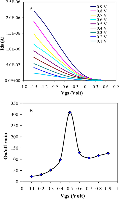
(A) I-V graph for the transfer characteristics. (B) Ion/Ioff ratio plot.
4 Conclusions
In this work, we have successfully demonstrated the fabrication step of CNT-FET. On the top of FET, drops containing different concentration of CNT were deposited, characterized, and analyzed. Increasing drops of CNT dispersion deposited on the sensing channel shows increasing conductivity of the fabricated CNT-FET. The conclusion drawn on the basis of observed transfer characteristics we find out that fabricated CNT-FET sensor showing p-type semiconductor property. Successfully achieve the CNT-FETs wafer fabrication with SWCNTs as the active semiconducting material between the source-drain electrodes by using the conventional photolithography method and lift-off techniques process. SEM analysis revealed that the presence of well-dispersed CNTs on the Si/SO2 surface. Single wafer with 84 CNT-FETs devices was fabricated and successfully characterized. After CNT-FETs device characterization it was found that 87% of the fabricated CNT-FETs were stable and functional. Among characterized CNT-FETs, 28% functional CNT-FETs have Ion/Ioff ratio larger than 25 while remaining 72% Ion/Ioff ratio falls under 25. The deviation of Ion/Ioff ratios in the CNT-FETs was mostly probably due to the contamination of CNT semiconducting material. However, the supplied CNTs are 99.9% pure semiconducting tubes or have very few tubes containing metal-based materials. As different variant of SARS-CoV-2 are being reported, this fabrication may be used for newly originated omicron and other pathogenic strains.
Funding
This work was supported by King Abdulaziz City for Science and Technology (General Directorate for Research & Innovation Support (GDRIS)) to King Abdulaziz University, Jeddah, Saudi Arabia to implement this work through fast track program for COVID-19 research project No. 5-20-01-009-0074.
Declaration of Competing Interest
The authors declare that they have no known competing financial interests or personal relationships that could have appeared to influence the work reported in this paper.
References
- Carbon nanotube - A review on synthesis, properties and plethora of applications in the field of biomedical science. Sensors Int.. 2020;1:100003
- [Google Scholar]
- Field-modulated carrier transport in carbon nanotube transistors. Phys. Rev. Lett.. 2002;89(12):126801
- [Google Scholar]
- Reversible sidewall functionalization of buckytubes. Chem. Phys. Lett.. 1999;310(3):367-372.
- [Google Scholar]
- Dispersion of single walled carbon nanotubes using a novel type of sonication: Focused sonication. J. Nanosci. Nanotechnol.. 2016;16(3):2836-2840.
- [Google Scholar]
- A meta-analysis of conductive and strong carbon nanotube materials. Adv. Mater.. 2021;33(36):2008432.
- [Google Scholar]
- Network single-walled carbon nanotube-field effect transistors (SWNT-FETs) with increased Schottky contact area for highly sensitive biosensor applications. J. Am. Chem. Soc.. 2006;128(7):2188-2189.
- [Google Scholar]
- Carbon nanotubes and graphene towards soft electronics. Nano Converg. 2014;1(1):15.
- [Google Scholar]
- A review of the interfacial characteristics of polymer nanocomposites containing carbon nanotubes. RSC Adv.. 2018;8(49):28048-28085.
- [Google Scholar]
- Incorporation of functionalized carbon nanotubes into hydrophobic drug crystals for enhancing aqueous dissolution. Colloids Surf. B Biointerfaces. 2019;173:386-391.
- [Google Scholar]
- Diameter control of single-walled carbon nanotube forests from 1.3-3.0 nm by arc plasma deposition. Sci. Rep.. 2014;4:3804.
- [Google Scholar]
- Mass production of high-purity semiconducting carbon nanotubes by hydrochloric acid assisted gel chromatography. ACS Appl. Nano Mater.. 2019;2(1):343-350.
- [Google Scholar]
- Critical challenges and advances in the carbon nanotube-metal interface for next-generation electronics. Nanoscale Adv.. 2021;3(4):942-962.
- [Google Scholar]
- Diminished band-gap transitions of single-walled carbon nanotubes in complexation with aromatic molecules. J. Am. Chem. Soc.. 2004;126(33):10234-10235.
- [Google Scholar]
- Directional alignment of carbon nanotubes in polymer matrices: contemporary approaches and future advances. Compos. A Appl. Sci. Manuf.. 2014;56:103-126.
- [Google Scholar]
- Determination of the surface coverage of exfoliated carbon nanotubes by surfactant molecules in aqueous solution. Langmuir. 2007;23(7):3646-3653.
- [Google Scholar]
- Morphological, rheological and electrical properties of composites filled with carbon nanotubes functionalized with 1-pyrenebutyric acid. Compos. B Eng.. 2018;147:12-21.
- [Google Scholar]
- Analytical prediction of highly sensitive CNT-FET-based sensor performance for detection of gas molecules. IEEE Access. 2020;8:12655-12661.
- [Google Scholar]
- Towards parallel fabrication of single electron transistors using carbon nanotubes. Nanoscale. 2015;7(21):9786-9792.
- [Google Scholar]
- Pharmaceutical characterization of solid and dispersed carbon nanotubes as nanoexcipients. Int. J. Nanomed.. 2012;7:403-415.
- [Google Scholar]
- Simple and cost-effective method of highly conductive and elastic carbon nanotube/polydimethylsiloxane composite for wearable electronics. Sci. Rep.. 2018;8(1):1375.
- [Google Scholar]
- Wrapping of self-organized fluorescent nanofibers with a silica wall. Langmuir. 2009;25(2):776-780.
- [Google Scholar]
- Dispersion, sedimentation and aggregation of multi-walled carbon nanotubes as affected by single and binary mixed surfactants. R. Soc. Open Sci.. 2019;6(7):190241
- [Google Scholar]
- Wafer-scale uniform carbon nanotube transistors for ultrasensitive and label-free detection of disease biomarkers. ACS Nano. 2020;14(7):8866-8874.
- [Google Scholar]
- Threshold voltage and on-off ratio tuning for multiple-tube carbon nanotube FETs. IEEE Trans. Nanotechnol.. 2009;8(1):4-9.
- [Google Scholar]
- Carbon nanomaterials field-effect-transistor-based biosensors. NPG Asia Mater.. 2012;4(8) e23–e23
- [Google Scholar]
- Carbon nanotubes in biology and medicine: In vitro and in vivo detection, imaging and drug delivery. Nano Res.. 2009;2(2):85-120.
- [Google Scholar]
- Supramolecular architectures of beta-cyclodextrin-modified chitosan and pyrene derivatives mediated by carbon nanotubes and their DNA condensation. J. Am. Chem. Soc.. 2008;130(31):10431-10439.
- [Google Scholar]
- Carbon nanotube-based electrochemical biosensing platforms: fundamentals, applications, and future possibilities. Recent Pat. Biotechnol.. 2007;1(2):181-191.
- [Google Scholar]
- Dispersion and functionalization of carbon nanotubes for polymer-based nanocomposites: A review. Compos. A Appl. Sci. Manuf.. 2010;41(10):1345-1367.
- [Google Scholar]
- Functionalized carbon nanotubes for probing and modulating molecular functions. Chem. Biol.. 2010;17(2):107-115.
- [Google Scholar]
- Biologically sensitive field-effect transistors: from ISFETs to NanoFETs. Essays Biochem.. 2016;60(1):81-90.
- [Google Scholar]
- Applications of carbon nanotubes-based biomaterials in biomedical nanotechnology. J. Nanosci. Nanotechnol.. 2006;6(7):1883-1904.
- [Google Scholar]
- Interaction of aromatic compounds with carbon nanotubes: Correlation to the Hammett parameter of the substituent and measured carbon nanotube FET response. Nano Lett.. 2003;3(10):1421-1423.
- [Google Scholar]
- Strength of carbon nanotubes depends on their chemical structures. Nat. Commun.. 2019;10(1):3040.
- [Google Scholar]
- Room-temperature transistor based on a single carbon nanotube. Nature. 1998;393(6680):49-52.
- [Google Scholar]
- Carbon nanotube assembly and integration for applications. Nanoscale Res. Lett.. 2019;14(1):220.
- [Google Scholar]
- Sonochemical degradation of N-methylpyrrolidone and its influence on single walled carbon nanotube dispersion. Chem. Commun.. 2015;51(93):16621-16624.
- [Google Scholar]
- How to make nanobiosensors: surface modification and characterisation of nanomaterials for biosensing applications. RSC Adv.. 2017;7(78):49386-49403.
- [Google Scholar]
- Carbon nanotube field-effect transistor (CNT-FET)-based biosensor for rapid detection of SARS-CoV-2 (COVID-19) surface spike protein S1. Bioelectrochemistry. 2022;143:107982
- [Google Scholar]