

Translate this page into:
Controlling the fabrication of sub-microgrooves on a silicon surface using a femtosecond laser
-
Received: ,
Accepted: ,
This article was originally published by Elsevier and was migrated to Scientific Scholar after the change of Publisher.
Peer review under responsibility of King Saud University.
Abstract
Altering the surface morphology is an approach that is commonly used to enhance desired properties. Femtosecond laser was used to fabricate sub-microgrooves at an average laser power of 31 mW with different scan speeds for a wavelength of 1026 nm. The effect of the laser wavelength on the sub-microstructure fabrication was also studied using 342 and 1026 nm wavelengths using spherical lens f = 40 mm with average powers of 9 mW and 25mW for UV and IR respectively. The sub-microgrooves had the same direction for horizontal, vertical, and diagonal scans. The fabricated sub-microstructures were investigated by a Field Emission Scanning Electron Microscope (FE-SEM) and an Atomic Force Microscope (AFM). At low scan speeds, sub-microgrooves did not appear because the number of pulses was too high. Thus, a high number of pulses per unit length can cause the sub-microgrooves to overlap, owing to the thermal effects. The overlap effects disappeared at scan speeds of 3 mm/s and higher. The sub-microgrooves length decreased as the scan speed increased. Separation distance and width increased with the scan speed. The separation distance reached a maximum value for the samples fabricated at a scan speed of 20 mm/s. At higher speeds, it decreased.
Keywords
Femtosecond laser
Sub-microfabrication
Silicon
Sub-microgrooves
Wavelength
FE-SEM
AFM

1 Introduction
Femtosecond-laser micro and nanostructuring have a wide range of applications in electronics, optoelectronics, surface and materials machining, and micro-electromechanical systems (MEMS). In sensing based MEMS, surface patterning plays a key role in increasing sensitivity because it creates trapping areas for the target molecules. Owing to the ultra-short pulse duration of femtosecond laser pulses, the time scale of electronic thermalization is around 100 fs; therefore, micro and nanostructures can be fabricated with small sidewall defects and high precision (Von der Linde et al., 1997; Sundaram and Mazur, 2002; He et al., 2016). Moreover, the diffraction limit can be overridden by the surface plasmon-laser interaction ablation, hence; femtosecond laser is a promising technique for manufacturing microscale devices with high accuracy (Huang et al., 2011, 2009). Nowadays, femtosecond-laser micromachining is used to fabricate various types of micro/nano structures on materials surfaces such as micro-grooves (Pan et al., 2013), periodical nanoripples (Tan and Venkatakrishnan, 2006), and microholes (Nasrollahi et al., 2018), in different environments, utilizing the control of laser parameters, e.g., repetition rate, laser power, wavelength, scan speed, and focusing lens (Ma et al., 2014). Laser-induced periodic surface structures on metals and semiconductors have been reported (Ulmeanu et al., 2012; Derrien et al., 2013; Oboňa et al., 2014; Bonse et al., 2013; Pan et al., 2016). The period of laser-induced nano structures (ʌ) is usually affected by the laser wavelength, the incident angle, and the material properties, according to Eq. (1) (Huang et al., 2009).
The objective of this work is to fabricate sub-microgrooves on the silicon surface and study the effect of the fabrication parameters on the microstructure and shape of the induced sub-microstructures. Such investigations are crucial for many structure related applications especially silicon based sensors where the microstructure is a key to achieve the sensitivity.
2 Experimental procedure
A laser micromachining system (Workshop of Photonics, Lithuania), consists of a PHAROS laser source linearly (horizontal) polarized laser with a fundamental wavelength of 1026 nm and pulse duration of 220 fs was used to illuminate the samples. The system included an optical path, a high-accuracy linear positioning stage, laser micromachining software SCA (Workshop of Photonics, Lithuania), and a machine-vision camera connected with the computer to monitor the fabrication processes. The original beam diameter of laser is 3.5 mm, focused by a 4X objective lens with a numerical aperture (NA) of 0.1 and a repetition rate of 100 kHz. The beam diameter (D) after focusing (at focus poin) is given by Eq. (5) (Huang et al., 2012).
The laser pulse energy was adjusted by a computerized attenuator. The material scanning speed, distance between two adjacent scanning lines, and number of scanning lines are set via the SCA software. The silicon wafer was fixed on a movable home stage, controlled by the computer program, and irradiated by the femtosecond laser. The microstructures were fabricated on the silicon wafer surface with high precision at different scan speeds (1, 2, 3, 5, 10, 20, 30, and 40 mm/s) at a power of 31 mW and focused by using 4× objective. The scan direction was adjusted by changing the direction of the transition stage. Third harmonic ultraviolet (342 nm) wavelength experiments were performed as well with an average laser power of 9 mW, a scan speed of 40 mm/s, and a spherical focusing lens with a focal length of 40 mm.
To remove the ablation-induced laser debris, the exposed silicon wafer was cleaned in a piranha solution for 5 min, then, rinsed by ethanol and distilled water, and dried at 250 °C for 10 min. Contaminants remaining on the surface were removed by cleaning the samples in an ultrasonic bath with acetone, ethanol, and deionized water for 10 min respectively. The microstructure of the irradiated samples was investigated by a Field Emission Scanning Electron Microscope (FE-SEM) and an Atomic Force Microscope (AFM).
3 Results and discussion
3.1 Structure of the fabricated sub-microgrooves
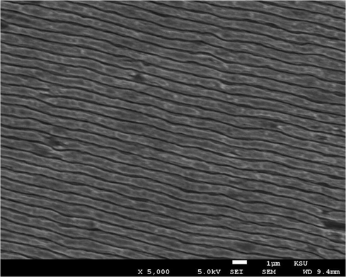
Fig. 2 shows the structure with a detailed morphology of the fabricated sub-mcrostructures by a single pass of the pulsed laser beam with 31 mW of power at scan speeds ranging from 1 mm/s to 40 mm/s, and the scan direction in the x-axis. The induced sub-microstructures have a ladder-like structure for samples prepared at scan speeds of 3, 5, 10, 20, 30, and 40 mm/s, as shown in Fig. 2(c–h). The periodic sub-microstructures were possibly obtained from the initial direct surface plasmon-laser interference and the subsequent grating-assisted surface plasmon-laser coupling (Huang et al., 2009; Oboňa et al., 2014). The first incident laser pulses on the surface create initial sub-microgrooves with periodicity near wavelength increased as the number of pulses decreases (Bonse et al., 2011, 2016, 2017; Huang et al., 2011, 2009). Since the initial sub-microgrooves deepen, the concentarion of the elctrons on the surface changes and resulted in the loss of the resonant Surface Plasmon Polariton (SPP) mode. Therefore, new electromagnetic mode appears with high electric field in the region between two initial sub-microgrooves. The high electric field causes damage in the area between initial sub-microgrooves which acts as seed for new sub-microgrooves, therefore new submicrogrooves will be formed (Huang et al., 2011; Bonse et al., 2017).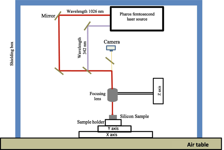
Diagram of femtosecond laser micromachining workstation from Femto-LAB (Workshop of Photonics).
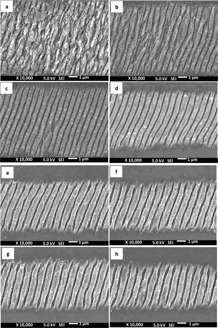
FE-SEM images for the induced sub-micro structures fabricated by femtosecond laser1026 nm wavelength focused by 4× with average power 31 mW and scan speeds (a) 1 mm/s (b) 2 mm/s (c) 3 mm/s (d) 5 mm/s (e) 10 mm/s (f) 20 mm/s (g) 30 mm/s (h) 40 mm/s.
Fig. 2(a) shows that, at low scan speeds, the ladder-like sub-microgrooves was destroyed. Sub-microgrooves appeared in the sample fabricated at the 2 mm/s scan speed; however, they overlapped, as shown in the SEM image in Fig. 2(b). Because the number of pulses per unit length applied on the surface of the material is high, which cause more splitting making the separation distance between two initial sub-microgrooves small. This resulted in overlapping of formed sub-microgrooves as illustrated in Fig. 2(b). On the other hand, at low scan speeds the thermal effects will not allow the formation of ultrafine gratings (Huang et al., 2011). Periodic sub-microgrooves appeared in the sample fabricated at 3 mm/s scan speed because the distance between the two pulses increased and number of pulses per unit length decreased, compared with the 1 and 2 mm/s scan speeds.
The length of the sub-microgrooves decreased with the increase of the scan speed. As illustrated in Fig. 3, the average length decreased from 8.86 µm to 5.31 µm for sub-microgrooves fabricated at scan speeds of 3 mm/s and 40 mm/s, respectively. The sub-microgroove length strongly depends on the scan speed because the energy per unit length increases with the scan speed according to Eq. (3) (Xue, A0097610E) hence, the spot diameter will be increased due to the increasing of the energy per unit length (Tshabalala et al., 2017).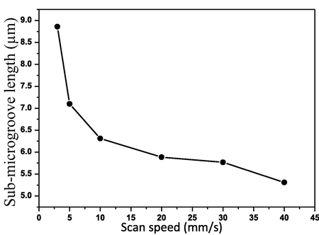
Sub-microgrooves length as function of scan speed fabricated by femtosecond laser1026 nm wavelength focused by 4× with average power 31 mW.
The separation distance between two sub-microgrooves and width of sub-microgrooves increase with the increase of scan speed as illustrated in Figs. 4 and 5. The separation distance between two sub-microgrooves increased with the scan speed and reached an optimum value of 534 nm for a sample fabricated at a 20 mm/s scan speed and decreased to 509 nm for a sample fabricated at a 40 mm/s. At low scan speeds the sub-microgrooves is deepened more and faster hence, the resonant SPP mode will be lost in shorter time therefore, the produced sub-microgrooves is narrower compared to that produced at higher scan speeds. The sub-microgrooves at low scan speed will be wider because the resonant SPP mode remain for more time causing more ablation on their edges hence the sub-microgrooves width is slightly increase with the increase of the scan speed (Huang et al., 2011). The separation distance between the two sub-microgrooves fabricated at scan speeds of 30 mm/s and 40 mm/s decreased due to the increasing of the sub-microgrooves width.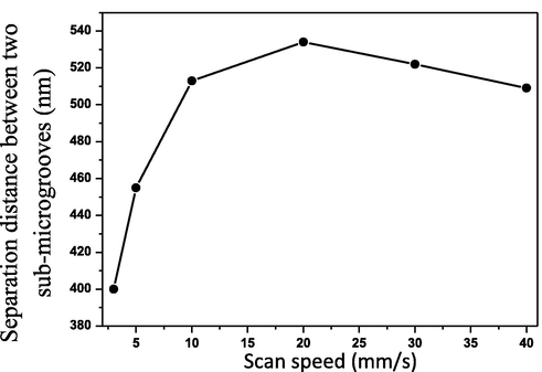
Separation distances between two sub-microgrooves as function of scan speed fabricated by femtosecond laser1026 nm wavelength focused by 4× with average power 31 mW.

Variation of sub-microgrooves width with scan speed fabricated by femtosecond laser1026 nm wavelength focused by 4× with average power 31 mW.
Figs. 6 and 7 show the 3D AFM images and depth for the induced sub-microgrooves fabricated at an average laser power of 31 mW and different scan speeds. The depth of the sub-microgrooves increases with the increasing of scan speed up to the maximum value at 30 mm/s. The decreasing of depth at lower scan speeds could be due to the redeposition of a significant amount of ablated particles on the sub-microgrooves (Le Harzic et al., 2014).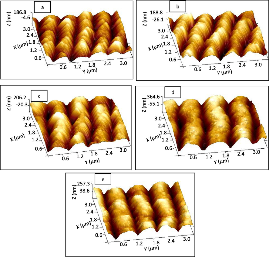
AFM images for the fabricated sub-microgrooves by femtosecond laser1026 nm wavelength focused by 4× with average power of 31 mW and scan speeds (a) 5 mm/s (b) 10 mm/s (c) 20 mm/s (d) 30 mm/s (e) 40 mm/s.
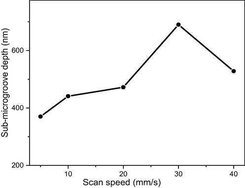
Depth of the fabricated sub-microgrooves by femtosecond laser 1026 nm wavelength focused by 4× with average power of 31 mW as function with san speed.
3.2 Effect of scan direction on orientations of the induced sub-microgrooves.
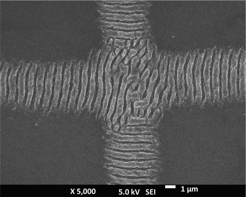
Fig. 8 illustrates the induced sub-microgrooves fabricated in different scan directions at an average power of 31 mW with a scan speed of 40 mm/s. The directions of the induced sub-microgrooves were the same for all scan directions, making 75° with the X-axis. As demonstrated in Fig. 8, each sub-microgroove has the same direction and independent of the scanning direction. Fig. 9 shows the orientations of the induced sub-microgrooves while the material is rotated and the scan direction is along the X-axis; it is clear that the direction of sub-microgrooves does not depend on the scan direction. The direction however depends on the polarization of the incident laser beam (Wagner et al., 2006; Bonse et al., 2016; Le Harzic et al., 2014). The polarization dependency of the induced ripples is related to the transverse magnetic characteristic of SPs (Huang et al., 2009). Fig. 10 illustrates the induced sub-microgrooves fabricated by the scanning of the sample surface in the x and y directions with separation distance between two laser beams of 7 µm with average power 31 mW and a scan speed of 40 mm/s. This phenomenon will be applied in the photo-nano fabrications beyond the diffraction limit and ful surface pattering.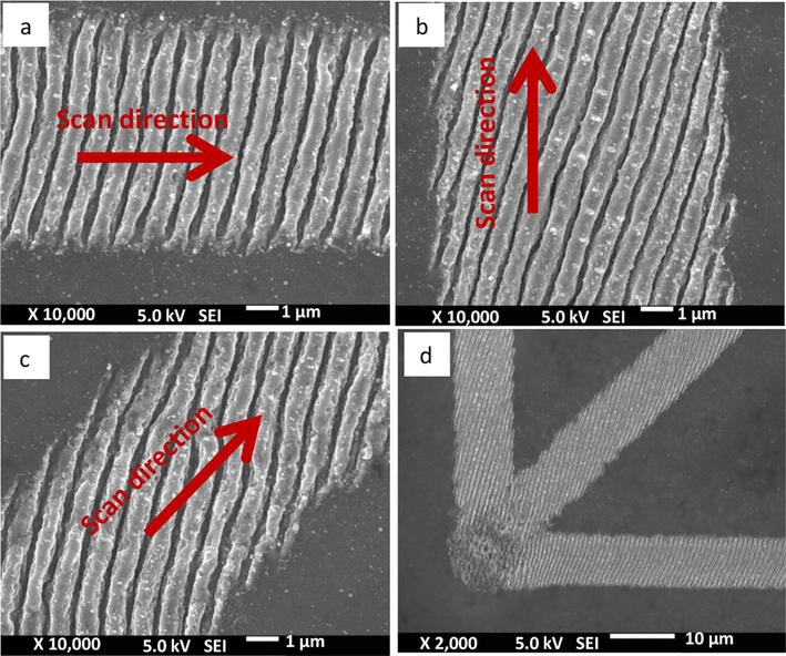
FE-SEM images for the sub-microgrooves fabricated by femtosecond laser 1026 nm wavelength focused by 4X with average power 31 mW and scan speed of 40 mm/s with different scan direction (a) horizontal (b) vertical (c) perpendicular (d) all previous three direction.
FE-SEM images for the sub-microgrooves fabricated by femtosecond laser 1026 nm wavelength focused by 4× with average power 31 mW and scan speed 40 mm/s with same scan directions and sample rotated 90°.
Vertical and horizontal lines with 7 µm separation distance between the centers of laser lines with average powe of 31 mW, and 1026 nm wavelength focused by 4×.
3.3 Effect of femtosecond laser wavelength on the shape of induced sub-microstructures
The effect of the laser wavelength on the morphology of the laser induced sub-microstructures on silicon surface were studied using an irradiate sample surface for a femtosecond laser with a wavelength of 342 nm. The sub-microstructure induced by a wavelength of 342 nm has sub-micro holes distributed within periodic groups as illustrated in Fig. 11(b). The separation distance between two groups is approximately 450 nm and the separation distance between two holes inside the individual group is 150 nm.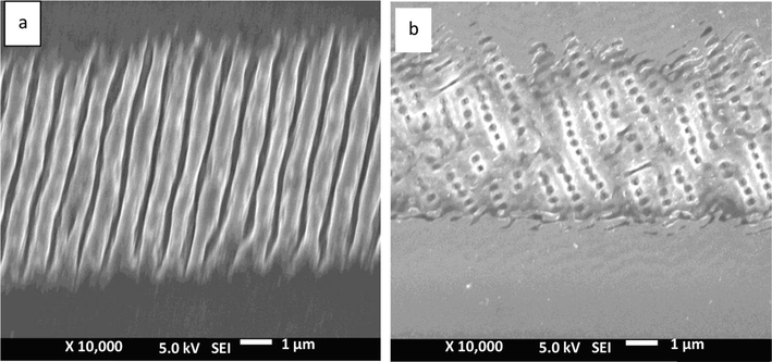
Femtosecond laser Induced nanostructures fabricated (a) 1026 nm wavelength and average power 25 mW (b) 342 nm wavelength, average power 9 mW. Beam Focused by spherical lens with focal length 40 mm.
4 Conclusion
In this work, we have shown that sub-microgrooves were successfully fabricated on the silicon surface by a femtosecond laser. The length of the sub-microgrooves decreased with the scan speed because of the decrease in the energy per unit length. The separation distance between two sub-microgrooves increased with the scan speed and was a maximum at 20 mm/s. It decreased for samples fabricated at scan speeds of 30 and 40 mm/s because of the laser–matter interactions. The width of the sub-microgroove increased with the scan speed; it increased from 157 nm to 276 nm for samples fabricated at scan speeds of 3 and 40 mm/s, respectively. The depth of the sub-microgrooves was measured by an AFM. The depth was decreased as scan speed decreased due to the redeposition of the significant amoun of the ablated particles at high number of pulses. The directions of the sub-microgrooves were independent of the scan direction and material orientations. The sub-microstructures fabricated by a laser with wavelength of 342 nm exhibited sub-micro holes structures. Finally, because of the surface plasmon-laser interactions, the scan speed strongly affected the fabricated sub-microgrooves at fixed average laser power and wavelength.
Acknowledgments
This research was funded by The Deanship of Scientific Research at King Saud University under the scientific program RG-1439-55. We thank the Deanship of Scientific Research and RSSU at King Saud University for their technical support.
Declaration of Competing Interest
The authors declare that they have no known competing financial interests or personal relationships that could have appeared to influence the work reported in this paper.
References
- Sub-100-nm laser-induced periodic surface structures upon irradiation of titanium by Ti: sapphire femtosecond laser pulses in air. Appl. Phys. A. 2013;110:547-551.
- [Google Scholar]
- Laser-induced periodic surface structures—A scientific evergreen. IEEE J. Sel. Top. Quant. Electron.. 2016;23(3)
- [Google Scholar]
- Implications of transient changes of optical and surface properties of solids during femtosecond laser pulse irradiation to the formation of laser-induced periodic surface structures. Appl. Surf. Sci.. 2011;257(12):5420-5423.
- [Google Scholar]
- Bonse, J., Kirner, S. V., Höhm, S., Epperlein, N., Spaltmann, D., Rosenfeld, A., & Krüger, J. (2017, February). Applications of laser-induced periodic surface structures (LIPSS). In Laser-based Micro-and Nanoprocessing XI (Vol. 10092, p. 100920N). International Society for Optics and Photonics.
- Possible surface plasmon polariton excitation under femtosecond laser irradiation of silicon. J. Appl. Phys.. 2013;114:083104
- [Google Scholar]
- Femtosecond laser high precision fabrication for novel applications. Curr. Nanosci.. 2016;12:676-684.
- [Google Scholar]
- Huang, H., Yang, L. M., & Liu, J., 2012. Direct welding of fused silica with femtosecond fiber laser. In Laser-Based Micro-and Nanopackaging and Assembly Vi. International Society for Optics and Photonics, 824403.
- Huang, M., Cheng, Y., Zhao, F., Xu, Z., 2011. Ultrafast laser-induced subwavelength structures towards nanoscale: the significant role of plasmonic effects. arXiv preprint arXiv:1109.6780.
- Origin of laser-induced near-subwavelength ripples: interference between surface plasmons and incident laser. ACS Nano. 2009;3:4062-4070.
- [Google Scholar]
- Cross-sectional study of high spatial frequency ripples performed on silicon using nanojoule femtosecond laser pulses at high repetition rate. Appl. Surf. Sci.. 2014;305:670-673.
- [Google Scholar]
- Progressive evolution of silicon surface microstructures via femtosecond laser irradiation in ambient air. Appl. Surf. Sci.. 2014;313:905-910.
- [Google Scholar]
- Drilling of micron-scale high aspect ratio holes with ultra-short pulsed lasers: critical effects of focusing lenses and fluence on the resulting holes’ morphology. Opt. Lasers Eng.. 2018;110:315-322.
- [Google Scholar]
- Pulse-analysis-pulse investigation of femtosecond laser-induced periodic surface structures on silicon in air. Opt. Express. 2014;22:9254-9261.
- [Google Scholar]
- Fabrication of two-dimensional periodic structures on silicon after scanning irradiation with femtosecond laser multi-beams. Appl. Surf. Sci.. 2016;368:443-448.
- [Google Scholar]
- Fabrication of high-aspect-ratio grooves in silicon using femtosecond laser irradiation and oxygen-dependent acid etching. Opt. Express. 2013;21:16657-16662.
- [Google Scholar]
- Inducing and probing non-thermal transitions in semiconductors using femtosecond laser pulses. Nat. Mater.. 2002;1:217-224.
- [Google Scholar]
- Tan Bo Xue. Device fabrication using femtosecond laser direct write method, thesis, National University of Singapore, A0097610E.
- A femtosecond laser-induced periodical surface structure on crystalline silicon. J. Micromech. Microeng.. 2006;16:1080.
- [Google Scholar]
- Surface texturing of SiAlON ceramic by femtosecond pulsed laser. Procedia Manuf.. 2017;7:660-667.
- [Google Scholar]
- Large scale microstructuring on silicon surface in air and liquid by femtosecond laser pulses. Appl. Surf. Sci.. 2012;258:9314-9317.
- [Google Scholar]
- Laser– solid interaction in the femtosecond time regime. Appl. Surf. Sci.. 1997;109:1-10.
- [Google Scholar]
- Wagner, R., Gottmann, J., Horn, A., Kreutz, E. W., 2006. Subwavelength ripple formation induced by tightly focused femtosecond laser radiation. Applied surface science, 252, 8576-85.