

Controlled magnetic behaviour of Ni80Fe20 nanowire by a selection of nucleation pads
⁎Corresponding author. hralqahtani@ksu.edu.sa (Hadi R. AlQahtani)
-
Received: ,
Accepted: ,
This article was originally published by Elsevier and was migrated to Scientific Scholar after the change of Publisher.
Peer review under responsibility of King Saud University.
Abstract
Magnetic nanowires are of technological importance as their magnetic properties can be controlled by their dimensions and shape. In soft magnetic nanowires (e.g. Ni 80 Fe 20 alloy or Permalloy), shape anisotropy has a very strong effect on their magnetic properties and thus the wire width and thickness control the domain patterns, nature of magnetization reversal, and the switching field. The switching field of a permalloy (Py) nanowire (NW) can be reduced substantially by attaching a microsized nucleation pad (NPD) to it. In this work, the OOMMF software package was used to perform micromagnetic simulations for selected NPD-NW structures. In this present study, we proved that the shape of the attached NPD is an important factor to consider. For instance, the switching field of structure comprises a triangular NPD (area = 0.25 μm2) with its head connected to a Py NW (20 nm wide) is about one fourth of the switching field of a square-like NPD-NW structure of the same size. Also the NPD size has an effect on the quality of the obtained hysteresis loop and thus it has to be comparable to the size of the NW for the sake of having a step-free hysteresis loop. These findings suggest that the rectangular NPD with its head connected to the NW may serve better than other shapes as it provides a directed motion for the domain walls to reach the NPD/NW interface easily. Thus it gives the highest reduction in the switching field of the Py nanowire in addition to a step-free hysteresis loop when the NPD size is 0.01 μm2.
Keywords
Nucleation pads
Ni80Fe20
Switching behaviour
Magnetic nanowires
Micromagnetic simulation
Oommf simulation

- DW
domain walls
- FDM
finite difference method
- FM
ferromagnetic
- LLG
Landau-Lifshitz-Gilbert
- NIST
National Institute of Standards
- NPD
nucleation pad
- NPD-NW
nucleation pad-nanowire structure
- NW
Nanowire
- OOMMF
Object Oriented Micromagnetic Framework
Abbreviations
1 Introduction
A recently-popularized research topic associated with nanoscale magnetism is that of controlling the magnetic properties of soft magnetic nanowires (NWs). Understanding the physical behaviors of domain walls (DWs) in planar ferromagnetic NWs is of technological importance as they can be employed in magnetic recording and in reading magnetic recording sensors (Nasirpouri and Nogaret, 2011). In addition, controlling domain-wall motion in magnetic nanowires by applying a magnetic or electric field could lead to the development of spintronic devices that can perform data storage and logic operations (Allwood et al., 2005; Parkin et al., 2008).
Due to their high aspect ratio (length/width ratio), Permalloy (referred to as Py or Ni80Fe20) nanowires have higher shape anisotropy compared to their thin film and nanoparticle counterparts. The term, higher shape anisotropy, means that the magnetic properties of a Ni80Fe20 NW are shape-dependent, and the magnetization is restricted to lying along the wire axis, and a single domain configuration becomes preferential (Ahmadi et al., 2019; Nasirpouri and Nogaret, 2011). In other words, the width and thickness of an Ni80Fe20 NW controls its domain patterns, the nature of its magnetization reversal, and consequently the switching field, that is, the field required to switch the magnetization between two opposite directions. The magnetization reversal of Ni80Fe20 NWs under the influence of a magnetic field usually occurs due to the nucleation and propagation of a single DW (Schrefl et al., 1997; Shigeto et al., 1999).
Moreover, it was found that the switching field of FM nanowires can be lowered significantly by attaching a micrometer-scale feature to the NW end (Schrefl, 1999; Shigeto et al., 1999). The reduced shape anisotropy of the microscale features (often termed nucleation pads (NPDs)) means that they reverse at lower fields compared with the wire, and then introduce a domain wall into the nanowire. These NPDs therefore reduce the switching field of the attached NW compared with the switching field of the free NW. Having a lower switching field than an isolated wire, the NPD works as a domain wall source. By applying a magnetic field along the wire axis, the domain walls are injected into the nanowire at the NPD/NW interface, where they experience pinning, after which they propagate once a critical field is reached (Cowburn et al., 2002; Schrefl, 1999; Shigeto et al., 1999). The choice of a rectangular NPD causes a step-like behavior in the hysteresis loop. This has been obtained experimentally at the interface of an NPD/NW structure (Cowburn et al., 2002). The step-like feature in the M−H loop is related to the fact that the NPD switches first, followed by the NW switching that is facilitated by the injection of a DW at a critical magnetic field.
Although NPDs have been known to be an effective method for controlling the switching field of soft magnetic nanowires for a while (Ahn et al., 2011; Bryan et al., 2010), there are some questions yet to be answered, such as what is the effect of changing the shape and size of the attached NPD on the quality of the obtained hysteresis loop of the NPD/NW combination. In the present study, we show that the shape and size of an NPD are of crucial importance in determining and controlling the magnetic behaviour of NPD/NW nanostructures.
2 Materials and methods
The nanowires in this study were designed using computer-aided design (AutoCAD) software (Autodesk, 2019). The micromagnetic simulations were carried out using the OOMMF package, which applies the finite difference method (FDM). FDM is considered to be one of the most suitable methods for simulating objects with rectangular (non-curved) geometries due to its higher performance and lower memory requirements compared to finite element modeling (Omari, 2016).
The OOMMF package is based on the Landau-Lifshitz-Gilbert equation (Kim, 2011):
Heff is the effective magnetic field (A/m), which is defined by:
where ∂E is the energy density. This consists of the following terms:
The LLG equation is a nonlinear differential equation and cannot be solved analytically for most geometries (Kim, 2011). Different types of solving methods are provided by OOMMF; among them is the mmSolve2D solver (Donahue, 2016). The simulation parameters for Ni80Fe20 are taken from Omari (2016) and can be listed as follows:
Saturation magnetization, Ms = 860 × 105 A/m,
Exchange stiffness, A = 1.3 × 10⁻¹¹ J/m,
Magnetocrystalline anisotropy constant
Damping constant,
The demagnetization was set as a constant, initial magnetization was to set to be random, and the anisotropy was chosen to be uniaxial. The total width, depth, and thickness values of the sample are also specified.
For this simulation, several masks containing our studied structures (several NPDs/ Ni80Fe20 NW structures) were designed using 2D AutoCAD software (Autodesk, 2019) as shown in Fig. 1. The Autodesk software’s resolution is in the range of 0.1 Angstrom, therefore we expect to have a negligible edge roughness. The selected shapes of the NPDs include squares, circles, triangles, and diamonds at fixed sizes: 0.01, 0.04, 0.09, 0.16 and 0.25 µm2. The sizes of these shapes were based on simple geometric calculations. The dimensions of the nanowire were kept fixed in all simulations: 1000 nm long, 20 nm wide, and 10 nm thick.
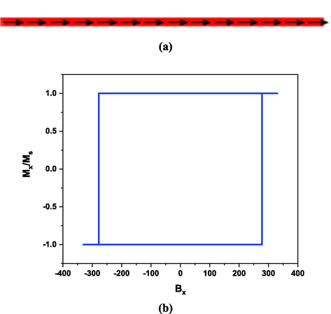
- (a) the magnetic configuration of a Ni80Fe20 nanowire (1000 nm long, 20 nm wide, 10 nm thick). (b) the hysteresis loop of the same nanowire.
We chose a cell size of 2 nm for the free nanowire simulation, but in order to speed up the simulation this was increased to 10 nm for the NPD/NW structures.
For the magnetostatic simulation, upon running the code, the magnetization state evolves until the structure reaches an equilibrium state (Kaya et al., 2016), where:
For the dynamic behavior study, the hysteresis loop for each structure was obtained by sweeping the applied field with a step size of 1 mT.
3 Results and discussion
Starting with a Ni80Fe20 nanowire (with dimensions of 1000 nm, 20 nm, and 10 nm) as shown in Fig. 1(a), the magnetostatic configuration gives a single domain structure pointing along the long axis due to the high shape anisotropy. The dynamic behavior of the Ni80Fe20 nanowire gives a perfect-square shaped hysteresis loop, which implies fast switching (Fig. 1(b)). The value of the switching field of the 20 nm wide Ni80Fe20 nanowire, as well as the coercive field, was found to be 278 mT (about 221 kA/m). The switching field of these narrow nanowires needs to be controlled so that it can be brought below 100 mT, in order to be easily implemented in future magnetic electronics.
To achieve precise control of the switching field of highly-reduced width (20 nm) Ni80Fe20 nanowires, we attached several nucleation pads of different shapes, sizes and areas. The static magnetic configurations at a zero applied field for the 0.25 µm2 nucleation pads of selected shapes attached to the Ni80Fe20 nanowire (with dimensions of 1000 nm, 20 nm, and 10 nm) are as shown in Fig. 2. As shown on the right-hand side of Fig. 2, each NPD comprises a multi-domain structure, whereas the nanowire has a single domain structure. The domain walls that are present in the nucleation pad are of a vortex-like structure. In the diamond-like shaped NPD, a more complex domain wall structure is observed. On the left-hand side, the energy densities for the exchange, magnetostatic (demag), and total energies are plotted versus the simulation time. The energy densities of all structures reach a minimum whenever stabilization starts to occur.
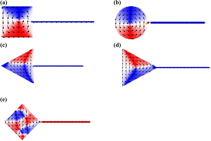
- The static magnetic configurations (at zero applied field) for the 0.25 µm2 nucleation pads of selected shapes of Ni80Fe20 NPDs connected to a Ni80Fe20 NW of fixed dimension. The shapes of the NPD include: a) square, b) circular, c) triangular (base connected), d) triangular (head connected) and e) diamond.
The magnetic energies: exchange, magnetostatic (demag) and total energy of all the selected structures are summarized in Table 1. The domination of the magnetostatic (demag) energy is evident for the free Ni80Fe20 NW, as the there is only a single domain structure. This causes the exchange to be at a minimum and the magnetostatic to be at a maximum. The addition of a nucleation pad should alter this by increasing the exchange and reducing the magnetostatic energy. It is also clear that the squared and circular NPD-NW structures have comparable values in terms of their exchange, magnetostatic, and total energies. This could be related to the same domain configuration present in the square and circular-like NPD-NW structures. The triangular NPD-NW structures (with either the base or the head facing the nanowire) have similar values for their magnetic energies; this is as a result of the same shape and magnetic configuration that is present in the triangular NPD-NW structures.
| Structure type | Exchange energy (J/m3) | Magnetostatics energy (J/m3) | Total energy (J/m3) |
|---|---|---|---|
| Single nanowire | 24 | 2948 | 2972 |
| Squared NPD-NW | 1670 | 1892 | 3563 |
| Circular NPD-NW | 1665 | 2280 | 3945 |
| Triangular NPD (base) – NW | 2183 | 4463 | 6647 |
| Triangular NPD (head) – NW | 2091 | 4095 | 6186 |
| Diamond NPD – NW | 6958 | 6296 | 13,254 |
However, we have found that the diamond-like shaped NPD-NW structure differs substantially in terms of total energy when compared with other structures in this study. This could be due to the complex domain wall configurations (double vortex-like configuration) that are present in the diamond-like shaped NPD-NW (Fig. 2e). The complex domain structure causes a significant increase in the exchange energy as a result of the increased number of domain walls in the structure, while higher demagnetizing energy means the structure has a higher shape anisotropy.
Moreover, we have studied the dynamic behavior of nucleation pad-nanowire combined structures as depicted in Fig. 3. The magnetic field was applied along the long axis of the nanowire (positive × direction). The resultant hysteresis loop structure is a combination of the hysteresis loop of the attached nucleation pad and the hysteresis loop of the nanowire. The nucleation pad, which works as a domain wall source, switches initially near the zero magnetic field as shown in the hysteresis loop (left-hand side of Fig. 3). The domain walls inside the nucleation pad can be injected into the nanowire. The injection needs a critical field, known as the injection field, to be accomplished. Unlike the dynamic behavior of the NPDs, the nanowire is characterized by fast switching once a domain wall is injected into the nanowire. It is well established that the magnetization reversal process in these NiFe nanostructures is controlled by nucleation (Cowburn, 2009).
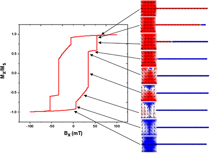
- Hysteresis loop of a squared NPD connected to the NW with the domain configuration taken at selected regions of the loop. The size of the nucleation pad is 0.25 μm2.
The hysteresis loops of the selected NPD-NW structures are shown in Fig. 4(a–e) for an NPD size of 0.01 µm2. The hysteresis curves varied from defected (the presence of step-like features) to non-defected (the absence of step-like features). As shown in Fig. 4a and d, the hysteresis loops of the square-like NPD-NW and the triangular (head connected) NPD-NW become smoother and non-defected at this selected size of these two nucleation pads. Other NPD shapes including circular, triangular connected from the base, and diamond failed to display defect-free hysteresis loops for all selected sizes of NPDs (as shown in Fig. 4(b, c, e)). The step-like behavior in the hysteresis loop is caused by the pinning of the domain walls at the NPD-NW interface, and/or at any sharp ends or corners. These effects are clearly seen in terms of the multi-steps that are present in the hysteresis loop of the diamond-like shaped NPD/NW structure. It is worth noting that a defect-free hysteresis loop is displayed when the size of the nucleation pad is comparable to the size of the nanowire, and when the domain walls are guided and injected into the NPD-NW interface. According to Kunz (2015), the diameter of the pad has to be kept small so that it contains a single domain, as the domain walls inside the pad.
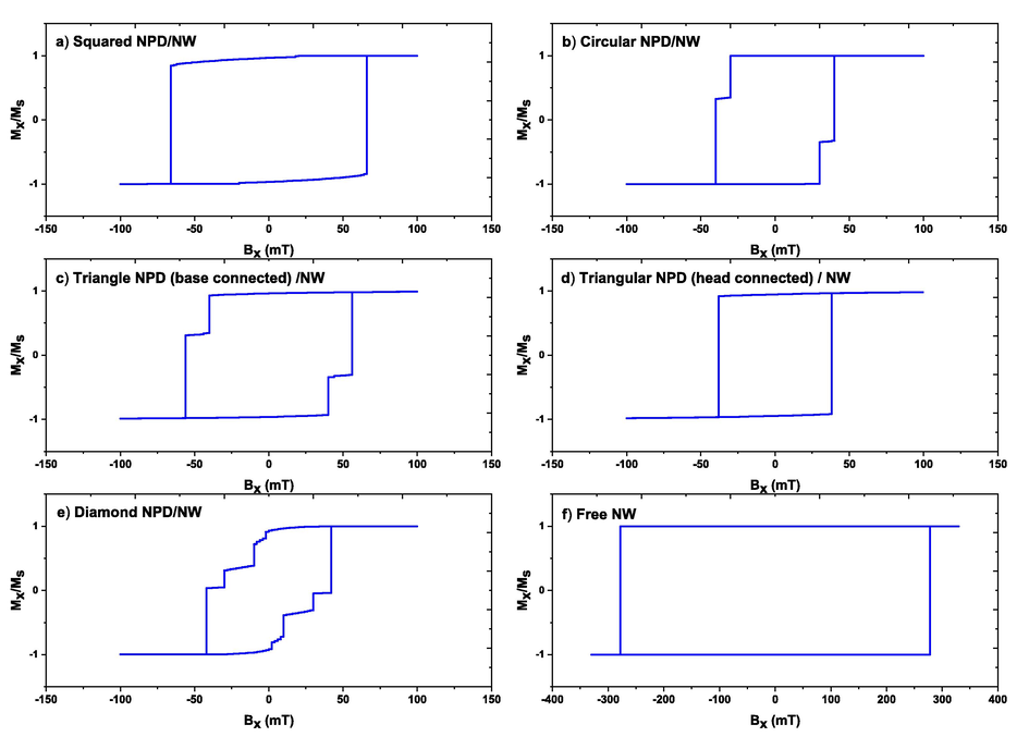
- The hysteresis loops of some selected Ni80Fe20 NPDs connected to a NW of the same material. The dimensions of the NW are fixed (1000 nm, 20 nm, 10 nm). The size of each NPD is 0.01 µm2. The selected shapes include: a) squared (Length = 100 nm), b) circular (radius (R) = 56.4 nm), c) triangular connected with base (base, B = 141.5 nm; height, H = 141.5 nm), d) triangular connected with head (B = 141.5 nm, H = 141.5 nm) and e) diamond (A = 141.5 nm, B = 141.5 nm). The last figure (f) represents the perfect square hysteresis loop for a free Ni80Fe20 NW for comparison.
The coercive field decays exponentially by increasing the nucleation-pad size for all structures as shown in Fig. 5(a). The exponential decay in coercivity as the size increases was seen in Han et al. (2009) and attributed to the magnetization reversal being changed from a pseudo-coherent rotation to nucleation.
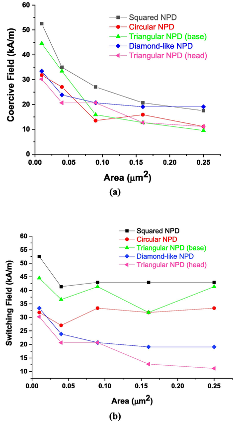
- The coercive field (a) and the switching field (b) vs. the size of some selected NPDs attached to a Ni80Fe20 nanowire of fixed dimension.
Furthermore, the switching field of each NPD-NW structure is drawn against the nucleation size as shown in Fig. 5(b). There are significant differences in the switching field among the studied structures. For instance, the switching field of the squared NPD-NW structure is almost twice that of the switching field of the triangular NPD connected to the head of the nanowire structure. The switching field of all structures depends on the shape and size of the attached nucleation pad, except in the case of the squared NPD-NW structure, where the size has no significant effect above 0.04 µm2. The squared NPD-NW structure was characterized by higher switching field values at all sizes of the nucleation pad, whereas the triangular NPD (head connected)-NW displayed the lowest values of the switching field at all sizes. This could be related to the directed motion of the domain wall in the triangular (head connected) NPD-NW structure, which enables it to find its way straightforwardly into the nanowire. In contrast, the domain wall in the squared NPD-NW structure experiences less directionality until it is eventually injected into the nanowire. The switching fields of the studied NPD-NW structures were analyzed and compared to the switching field of a single nanowire (free NW). At the maximum NPD size (A = 0.25 μm2), the switching field of the triangular (head) NPD-NW structure was the lowest (Hs = 14 mT causing a 95% reduction in the switching field of the single nanowire structure) while the diamond-like shaped NPD-NW structure came second (Hs = 24 mT => 91.4% switching field reduction compared to a similar nanowire with no attachment). The domain walls in these two structures can be easily guided by the geometry to reach the NPD/NW interface (higher directionality).
The circular NPD-NW structure comes third with an approximately 88.5% reduction in the switching field compared to the single-nanowire structure. The square-like and triangular (base connected) NPD-NW structures have comparable switching-field values (approximately 81.3% and 85.6% respectively) suggesting less directionality for the domain wall to reach the nanowire entrance in these two structures. An important finding in terms of the significance of the chosen shape of the NPD is that the switching field of the squared NPD-NW structure is almost four times the value (Hs) that is obtained for the triangular (head connected) NPD-NW structure at the maximum NPD size (0.25 µm2). Therefore, these two geometries of NPD-NW structures can be used in spintronic applications (e.g. the fabrication of planar-spin valves (Alqahtani et al., 2014)).
4 Conclusion
The effect of the shape and size of some selected Ni80Fe20 NPDs on the magnetic properties of Ni80Fe20 NPD/NW structure was investigated. The reduction in the coercive and switching fields of NPD/NW structures depends on the shape of the attached NPD. The highest reduction is observed when using triangular (connected from the head) and diamond-like shaped NPDs. These shapes enable a sort of guidance for the domain wall to reach the NPD/NW interface. The size is also a critical factor in terms of obtaining a defect-free hysteresis loop for the Ni80Fe20 NPD/NW structure. The size of the NPD should be comparable to the size of the nanowire in order to obtain a defect-free hysteresis loops in the squared and triangular NPD (head connected)-NW structures. These NPD/NW structures may be employed in spintronic applications (e.g. in co-planar spin valves).
Acknowledgements
This project was supported by King Saud University, Deanship of Scientific Research, College of Science Research Center.
Declaration of Competing Interest
The authors declare that they have no known competing financial interests or personal relationships that could have appeared to influence the work reported in this paper.
References
- Control of domain-wall injection field with different nucleation pad geometry. J. Nanosci. Nanotechnol.. 2011;11:6476-6478.
- [CrossRef] [Google Scholar]
- Planar organic spin valves using nanostructured Ni80Fe 20 magnetic contacts. Org. Electron.. 2014;15:276-280.
- [CrossRef] [Google Scholar]
- Autodesk, 2019. AutoCAD For Mac & Windows | CAD Software | Autodesk. https://www.autodesk.com/
- Transverse field-induced nucleation pad switching modes during domain wall injection. IEEE Trans. Magn.. 2010;46:963-967.
- [CrossRef] [Google Scholar]
- Cowburn, R.P., 2009. Magnetic nanowires for domain wall logic and ultrahigh density data storage, in: Nanoscale Magnetic Materials and Applications. Springer, pp. 219–236. https://doi.org/10.1007/978-0-387-85600-1_8
- Domain wall injection and propagation in planar Permalloy nanowires. J. Appl. Phys.. 2002;91:6949-6951.
- [CrossRef] [Google Scholar]
- Donahue, M.J., 2016. OOMMF user’s guide, version 1.2b0. https://doi.org/10.6028/nist.ir.6376.
- Han, N., Guo, G., Zhang, L., Zhang, G., Song, W., 2009. Magnetization reversal for Ni nanowires studied by micromagnetic simulations. J. Mater. Sci. Technol. 25, 151. https://www.jmst.org/EN/Y2009/V25/I02/151
- Nucleation and interactions of 360∘ domain walls on planar ferromagnetic nanowires using circular magnetic fields. AIP Adv.. 2016;6:55025.
- [CrossRef] [Google Scholar]
- Magnetization Dynamics in a Permalloy Disc and Nanowire. Konstanz: University of Konstanz; 2011. PhD thesis
- Low-field magnetic domain wall injection pad and high-density storage wire. US patents, US. 2015;9,196,280:B2.
- [Google Scholar]
- Nasirpouri, F., Nogaret, A., 2011. Nanomagnetism and Spintronics: Fabrication, Materials, Characterization and Applications. World Scientific. https://doi.org/10.1142/7281
- Understanding and Controlling Dynamically-Induced Stochastic Domain Wall Behaviours in Magnetic Nanowires. Sheffield: University of Sheffield; 2016. PhD thesis
- Finite elements in numerical micromagnetics: Part ii: patterned magnetic elements. J. Magn. Magn. Mater.. 1999;207:66-77.
- [CrossRef] [Google Scholar]
- Domain structures and switching mechanisms in patterned magnetic elements. J. Magn. Magn. Mater.. 1997;175:193-204.
- [CrossRef] [Google Scholar]
- Injection of a magnetic domain wall into a submicron magnetic wire. Appl. Phys. Lett.. 1999;75:2815-2817.
- [CrossRef] [Google Scholar]