Translate this page into:
Annealing effects on the structural, electrical and optical properties of ZnO thin films prepared by thermal evaporation technique
⁎Corresponding author at: Department of Pharmacy, Faculty of Medicine, University of Constantine 3, Algeria. zaier_abdelhakim@yahoo.fr (A. Zaier)
-
Received: ,
Accepted: ,
This article was originally published by Elsevier and was migrated to Scientific Scholar after the change of Publisher.
Peer review under responsibility of King Saud University.
Abstract
Zinc oxide (ZnO) thin films have been prepared on glass substrates at room temperature by thermal evaporation technique using ZnO powders and then are annealed at different temperatures ranging from 200 °C to 500 °C for 2 h in air. The effect of the annealing temperature (Tr) on the structural, optical and electrical properties of the ZnO thin films was studied.
Experimental results show that annealing temperature has an important role in the changes observed in the structural, optical and electrical properties of the ZnO thin films. The XRD measurements confirm that the thin films grown by this technique have good crystalline hexagonal wurtzite structures. The optical transmittance spectra show transmittance higher about ∼90% within the visible wavelength region. Hence, the values of the gap are found to be between 3.13 and 3.25 eV. The resistivity values of the films have changed between 2.10−3 and 4.10−2 Ω cm with annealing temperature.
Keywords
Thin films
Zinc oxide (ZnO)
Thermal evaporation
Annealing temperature
1 Introduction
Zinc oxide (ZnO) is a wide-band gap n-type semiconductor of the II–VI semiconductor group with a zinc excess in interstitial position. It is currently the subject of numerous studies because of its exceptional properties, such as more elevated chemical and thermal stability even in atmosphere of hydrogen plasma compared to other oxides (SnO2, ITO), large exciton binding energy of 60 meV at room temperature, non-toxicity and its low price (Volkan et al., 2014; Chrissanthopoulos et al., 2011; Mimouni et al., 2015), which allow it to be like a material model especially in its extremely various applications (electronics, optics, optoelectronics, conversion photovoltaic) (Chuen et al., 2012; Djurisic et al., 2010; Al-Hardan et al., 2014; Keun et al., 2013). ZnO thin films have been prepared by various techniques such as thermal evaporation (Chrissanthopoulos et al., 2011; Ghislain et al., 2013; Yuvaraj et al., 2008; Feng et al., 2010; Nguyen et al., 2014), Pulsed laser deposition (Raied et al., 2014), molecular beam epitaxy (Zhang et al., 2011), magnetron sputtering (Ismail and Abdullah, 2013; Mosbah and Aida, 2012), sol–gel (Hashim et al., 2013; Linhua et al., 2012), chemical vapour deposition (Hsiao et al., 2013; The-Long et al., 2010; Jeon et al., 2014) and spray pyrolysis (Zaier et al., 2009; Lucio et al., 2006). Thermal evaporation is an interesting technique because of its simple process of deposition, films uniformity and mainly species evaporation controllability. The present work deals with ZnO thin film deposition using thermal evaporation. The structural, optical and electrical properties of the films were studied as a function of annealing temperature.
2 Experimental
ZnO thin films, used in this study, were deposited onto glass substrates at room temperature by thermal evaporation technique using ZnO powders (99.99% purity). The distance between Substrate to source was 6 cm. The base pressure in the deposition chamber was evacuated to 10–5 mbar. The source current was increased slowly (up to 3 A) and the vapour species condenses onto glass substrates. After deposition, these films were followed by thermal oxidation in air using furnace Linn High Therm GmbH (Model LM 312) at various temperatures ranging from 200 °C to 500 °C for a fixed time of 2 h. The films structural characterisation was carried out using X-ray diffraction (ray Kα1 of the Cu, λ = 1.5405 Å) system. Films thickness was measured by Dektak profilometry. For the optical properties measurements, we used a double beam Shimadzu 1700 UV–vis spectrophotometer with an integrating sphere in the wavelength range from 200 to 1100 nm. The electrical properties measurements were performed with four probe method.
3 Results and discussion
3.1 Structural properties
Fig. 1 shows the recorded XRD diffraction pattern of ZnO samples deposited by thermal evaporation technique and annealed at different temperatures. This result clearly shows that ZnO thin film is polycrystalline hexagonal wurtzite structure (according to JCPDS card No. 00-036-1451), these results were found by Raied et al. (2014). Strong (0 0 2) preferential orientation indicates polycrystalline nature of the thin films ZnO.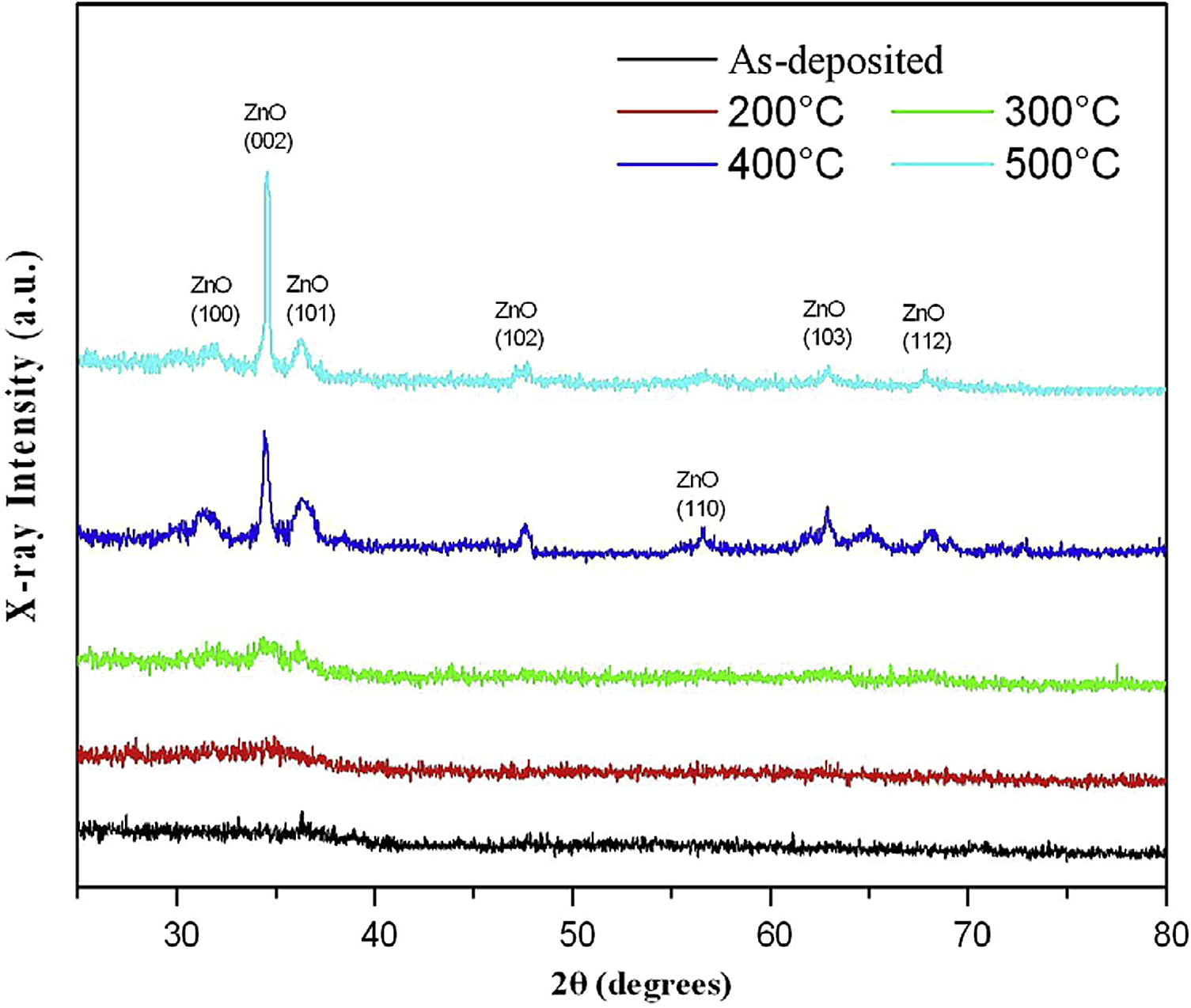
XRD patterns of ZnO thin films annealed at various temperatures.
The crystallite size of the ZnO thin films was calculated by using the Debye–Scherrer formula (Hosseinmardi et al., 2012):
Fig. 2 shows ZnO diffraction peak (0 0 2) full width at half-maximum (FWHM) and mean grain size as a function of the annealing temperatures (Tr). With elevating annealing temperature the film’s mean grain size increases, and FWHM of the (0 0 2) peak becomes narrower indicating the improvement of the crystalline of ZnO.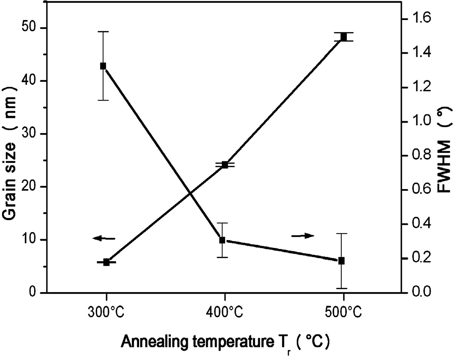
FWHM of the main XRD peak and corresponding grain sizes of ZnO films as a function of the annealing temperature.
3.2 Optical properties
The optical transmittance spectra with wavelengths from 320 to 900 nm ZnO films annealed for different temperatures are presented in Fig. 3. Optical transmission increases according to the annealing temperature from 200 °C to 500 °C until a value of 90% for the films annealing at 500 °C, because of structural homogeneity, crystallinity and the thicknesses of films, as reported by Hamid et al. (2007).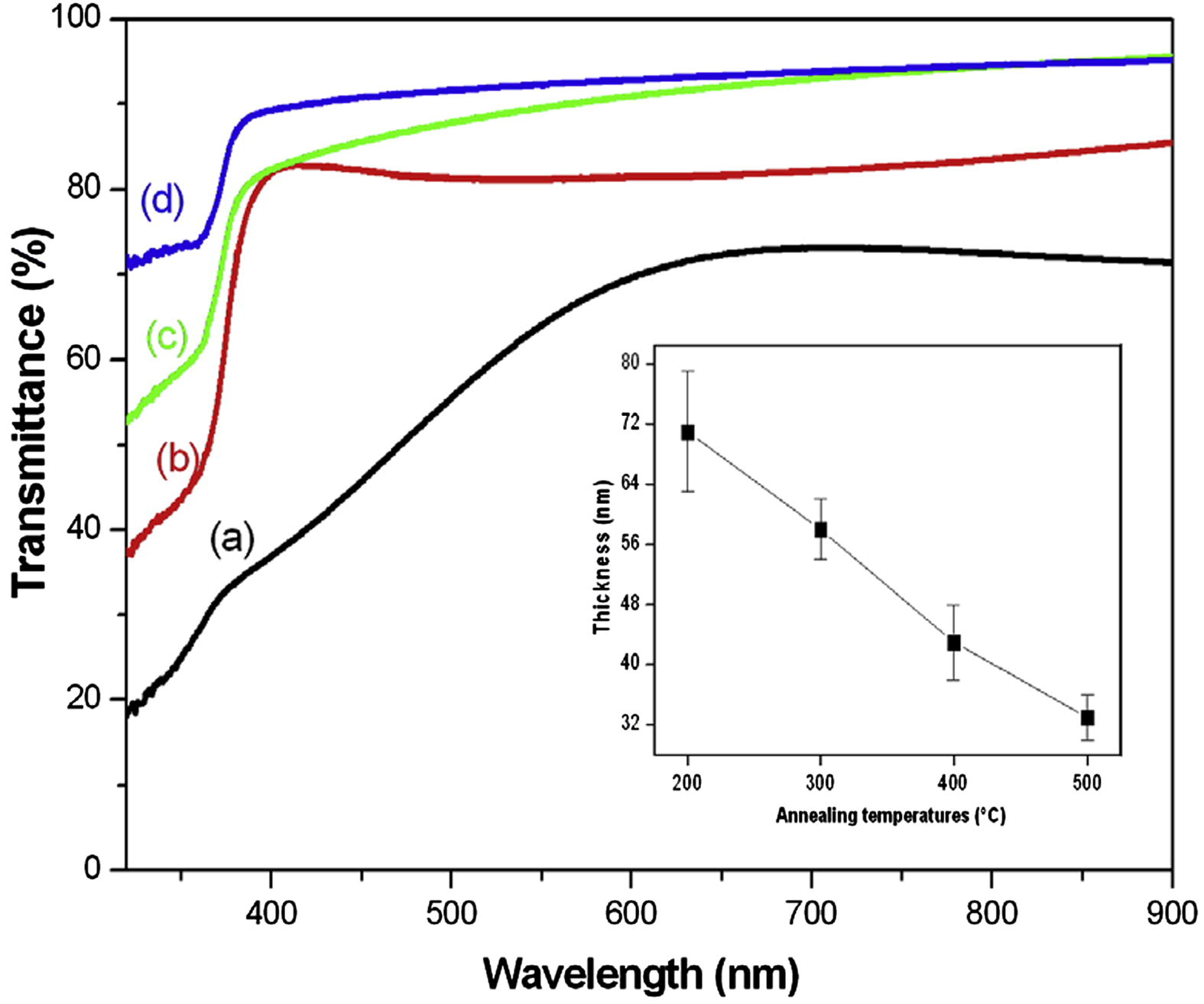
The transmission (%) spectra of ZnO thin film annealed at different temperatures (Tr): (a) 200 °C, (b) 300 °C, (c) 400 °C, and (d) 500 °C. The inset shows the films thickness variation of different annealed temperatures.
The band gap of the films corresponding to annealing temperature for 200–500 °C was calculated by plotting (αhν)2 vs hν using the relation (Ayouchi et al., 2003):
The energy gap (Eg) value is calculated by extrapolation of the straight line of the plot of (αhν)2 versus photon energy (hν) for the different annealing temperatures, are shown in Fig. 4. The energy band gap increases with the annealing temperature. It varies from 3.13 eV to 3.25 eV for 200 °C to 500 °C annealing temperatures, respectively. These values of the band gap are in agreement with those found by Malek et al. (2014). This change in energy band gap can be attributed to the reduction of the structural defects in films network and also to the increase of grain size with annealing.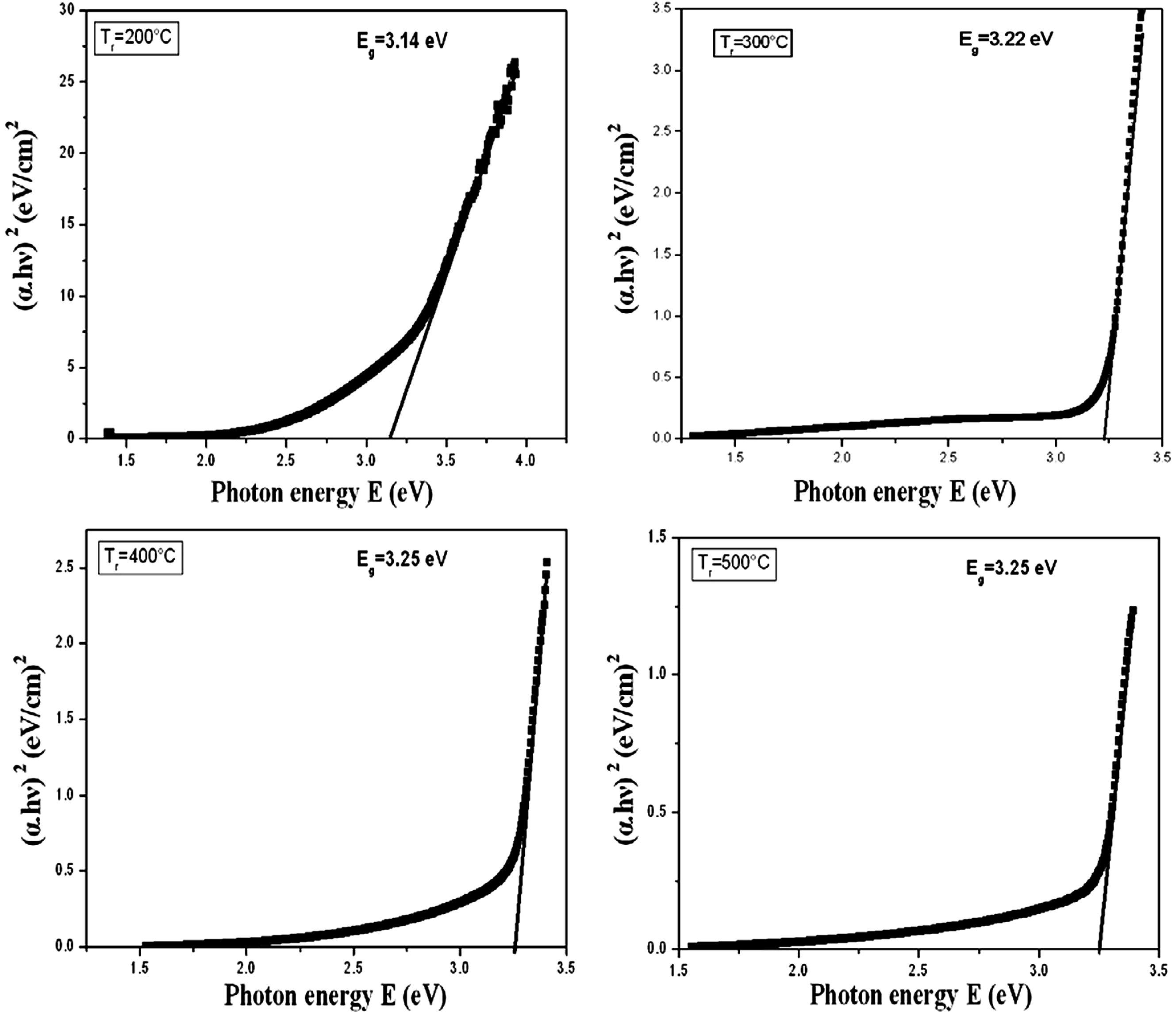
The plot of (αhν)2 versus photon energy (hν) for ZnO thin films prepared at various temperatures (Tr).
3.3 Electrical properties
The resistivity of the films is calculated using the following equation: where: d: is the thickness of the sample, V: is the voltage and I: is the current. K: is a constant dependent on the geometry is equal with .
The resistivity variation with annealing temperature of the ZnO films is shown in Fig. 5. As can be seen, the resistivity increases with annealing temperature from 2.10−3 to 4.10−2 Ω cm for 0 °C (As deposited) and 500 °C respectively. This can be attributed to the increase of oxygen when increasing the annealing temperature that reduces the number of oxygen vacancies (free carrier) in ZnO films. Asghar et al. (2008) and Bouhssira et al. (2006) have reported similar results.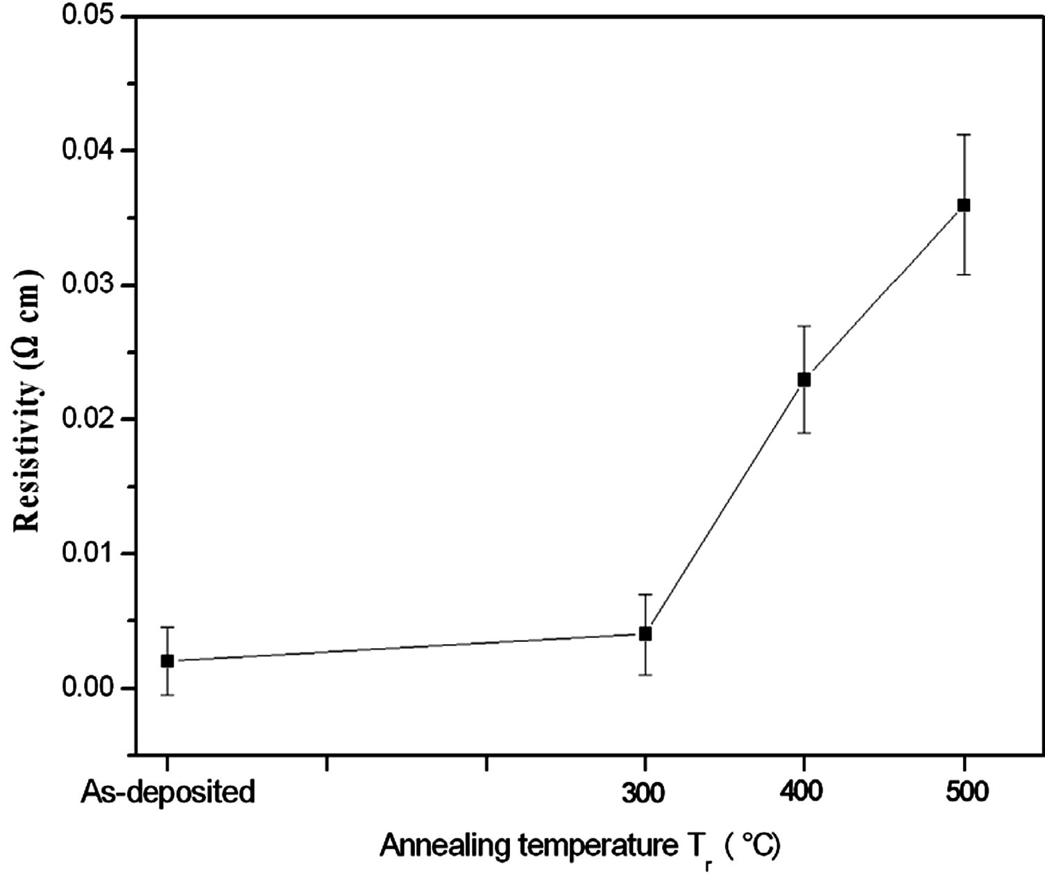
Variation of the electrical resistivity with the annealing temperature.
4 Conclusion
In summary, ZnO thin films have been deposited by thermal evaporation method on glass substrates. The films have been annealed in a furnace at different temperatures. The XRD results reveal that the deposited thin film has a good polycrystalline hexagonal wurtzite structure. The size of crystalline (grains) for annealing at 500 °C is about 1.5 nm. The average transmittance in visible region is about ∼90% increasing with annealing temperature. The optical band gap of ZnO films is in the range of 3.13–3.25 eV. The more the electrical resistivity of the films increases, the more the annealing temperature rises. Finally, we can say that we have prepared samples of ZnO of good optical and electrical properties which can be used in many opto-electrical applications and mainly in the field of photovoltaic cells.
Acknowledgments
The authors would like to thank Dr. A. Ayad, Laboratory of Microstructures and Defects in Materials, Constantine University 1 – Algeria, for his help in the DRX characterization.
References
- Preparation and characterization of transparent ZnO thin films obtained by spray pyrolysis. Thin Solid Films. 2003;426:68-77.
- [Google Scholar]
- Post-annealing modification in structural properties of ZnO thin films on p-type Si substrate deposited by evaporation. Sci. Semicond. Process.. 2008;11:30-35.
- [Google Scholar]
- A wide-band UV photodiode based on n-ZnO/p-Si heterojunctions. Sens. Actuators A. 2014;207:61-66.
- [Google Scholar]
- Influence of annealing temperature on the properties of ZnO thin films deposited by thermal evaporation. Appl. Surf. Sci.. 2006;252:5594-5597.
- [Google Scholar]
- Synthesis and characterization of ZnO/NiO p–n heterojunctions: ZnO nanorods grown on NiO thin film by thermal evaporation. Photonics Nanostruct. Fundam. Appl.. 2011;9:132-139.
- [Google Scholar]
- The effect of ZnO-coating on the performance of a dye-sensitized solar cell. Sol. Energy. 2012;86:1435-1442.
- [Google Scholar]
- ZnO nanostructures for optoelectronics: material properties and device applications. Prog. Quantum Electron.. 2010;34:191-259.
- [Google Scholar]
- Fabrication and characterization of tetrapod-like ZnO nanostructures prepared by catalyst-free thermal evaporation. Mater. Charact.. 2010;61:128-133.
- [Google Scholar]
- Synthesis of ZnO nanostructure films by thermale vaporation approach and their application in dye-sensitized solar cells. Mater. Sci. Semicond. Process.. 2013;16:652-658.
- [Google Scholar]
- Fabrication and characterization of ZnO thin film using sol–gel method. Opt. Int. J. Light Electron. Opt.. 2013;124:491-492.
- [Google Scholar]
- Highly textured ZnO:B films grown by low pressure chemical vapor deposition for efficiency enhancement of heterojunction silicon-based solar cells. J. Taiwan Inst. Chem. Eng.. 2013;44:758-761.
- [Google Scholar]
- A study on the photoluminescence properties of electrospray deposited amorphous and crystalline nanostructured ZnO thin films. Ceram. Int.. 2012;38:1975-1980.
- [Google Scholar]
- The effect of annealing on structural, electrical and optical properties of nanostructured ITO films prepared by e-beam evaporation. Mater. Res. Bull.. 2007;42:487-496.
- [Google Scholar]
- The structural and optical properties of ZnO thin films prepared at different RF sputtering power. J. King Saud Univ. Sci.. 2013;25:209-215.
- [Google Scholar]
- Enhanced mobility of Li-doped ZnO thin film transistors fabricated by mist chemical vapor deposition. Appl. Surf. Sci.. 2014;301:358-362.
- [Google Scholar]
- Highly conductive and damp heat stable transparent ZnO based thin films for flexible electronics. J. Alloys Compd.. 2013;554:240-245.
- [Google Scholar]
- Dependence of structural and optical properties of sol–gel derived ZnO thin films on sol concentration. Appl. Surf. Sci.. 2012;258:7760-7765.
- [Google Scholar]
- Preparation of conducting and transparent indium-doped ZnO thin films by chemical spray. Sol. Energy Mater. Sol. Cells. 2006;90(6):733-741.
- [Google Scholar]
- Influence of deposition temperature on structural, optical and electrical properties of sputtered Al doped ZnO thin films. J. Alloys Compd.. 2012;515:149-153.
- [Google Scholar]
- Investigation of structural and optical properties in Cobalt–Chromium co-doped ZnO thin films within the Lattice Compatibility Theory scope. J. Alloys Compd.. 2015;624:189-194.
- [Google Scholar]
- Thermal annealing-induced formation of ZnO nanoparticles: minimum strain and stress ameliorate preferred c-axis orientation and crystal-growth properties. J. Alloys Compd.. 2014;610:575-588.
- [Google Scholar]
- Near-infrared emission from ZnO nanorods grown by thermal evaporation. J. Lumin.. 2014;156:199-204.
- [Google Scholar]
- Optical properties of nanostructured ZnO prepared by a pulsed laser deposition technique. Mater. Lett.. 2014;132:31-33.
- [Google Scholar]
- Photoluminescence properties of various CVD-grown ZnO nanostructures. J. Lumin.. 2010;130:1142-1146.
- [Google Scholar]
- ZnO thin film synthesis by reactive radio frequency magnetron sputtering. Appl. Surf. Sci.. 2014;318:2-5.
- [Google Scholar]
- Optical and electrical properties of ZnO films deposited by activated reactive evaporation. Vacuum. 2008;82:1274-1279.
- [Google Scholar]
- Effects of the substrate temperature and solution molarity on the structural opto-electric properties of ZnO thin films deposited by spray pyrolysis. Mater. Sci. Semicond. Process.. 2009;12(6):207-211.
- [Google Scholar]
- Realization of non-polar ZnO (1120) homoepitaxial films with atomically smooth surface by molecular beam epitaxy. J. Cryst. Growth. 2011;325:93-95.
- [Google Scholar]


