

Translate this page into:
Analysis of gamma dose dependent nanostructure, morphological, optical and electrical properties of CeO2 thin films
⁎Corresponding author. Sdawood@ksu.edu.sa (S. Aldawood)
-
Received: ,
Accepted: ,
This article was originally published by Elsevier and was migrated to Scientific Scholar after the change of Publisher.
Peer review under responsibility of King Saud University.
Abstract
The structural, morphological, optical and electrical properties of CeO2 thin films deposited on glass substrate using spin coating technique are studied with and without gamma irradiation. The prepared samples were gamma irradiated with 60Co at room temperature with dose range from 0 to 100 kGy. The pristine and gamma exposed samples were analyzed by X-ray diffraction (XRD), field emission scanning electron microscope (FESEM), energy dispersive X-rays (EDX), UV–Vis Spectroscopy, photoluminescence (PL) and Hall measurements. XRD results confirmed the face-centered cubic phase of CeO2 for all samples and showing the decreased in the crystallinity with gamma irradiation dose values. The FESEM images shows that after gamma exposure, the CeO2 thin films surface became compressed, smooth and uniform. UV–Vis Spectroscopy determined that the shifting of energy band gap values accredited by creating or eradication of induced defects inside the energy band gap. PL peaks appeared in pristine and irradiated thin films can be allocated to the oxygen related defects. The mobility, electrical resistivity and carrier concentration were estimated for all sample by Hall measurements. It was found that the electrical properties, such as an increase in the number of carrier concentration and the decrease in the resistivity, of the CeO2 thin films were improved with gamma rays irradiation. The study successfully demonstrates that CeO2 thin films is a potential candidate to detect gamma radiation for dosemetric application.
Keywords
Gamma irradiation
XRD
Energy band gap
Photoluminescence
Hall measurements

1 Introduction
In the last decades, to develop new radiation dosimeters in place of aqueous chemical dosimetry, a numerous effort has been reported to examine the impact of irradiation on the characteristics of metal oxide semiconductor (Manikanthababu et al., 2020, Rabia, 2017; Manikanthababu et al., 2019). Among the metal oxide semiconductor, cerium oxide (CeO2) has received more attention because of its high band gap, large refractive index, good temperature stability, high dielectric constant and excellent optical response. As detecting/sensing material, CeO2 has been found in many aspects, like gas detector (Abouda et al. 2018), ultraviolet radiation sensor (Wu et al. 2019), temperature sensors (Sun et al. 2012), humidity sensors (Li et al. 2015) and radiation sensor (Tugulan and Ioan, 2020; Zohdiaghdam et al. 2020).
Gamma radiation has high frequency, which allow it to deeply penetrate inside of a matter depending on its energy. So, gamma rays may induce some effects to the encountered material , such as excitation of electron, ionization of material and atomic movement of the orbited electrons (Pacchioni et al., 2000). These effects are reason the structural defects (oxygen deficiency in oxides semiconductor) and change in their density (Trefilova et al. 2001; Zhu, 1998). The nature of these defects depend on the electronic structure of material and the radiation dose (Pacchioni et al., 2000). The behavior of CeO2 thin film with gamma irradiation was studied by Yingying Li (Li et al. 2009) and reported that the optical properties of CeO2 nanowire are clearly influenced by gamma irradiation. Furthermore, electrochemical properties demonstrated the CeO2/graphene junction under a gamma irradiation environment (Xia et al. 2017). The previous results indicate that the dosimetric behavior of CeO2 could endure without any significant variations in the device functionality.
The purpose of the present work is to explore the influence of gamma irradiation with different dose on the nanostructure, morphological, optical and electrical properties of nanocrystalline CeO2 thin films for gamma sensing martials. To our best knowledge, there is no comprehensive investigation in the literature about the gamma induced detailed behavior of CeO2 thin films deposited by spin coating method.
2 Methods and techniques
2.1 Thin film deposition
Sample preparation: The cerium dioxide (CeO2) films on the glass substrate were prepared by mixing of 0.5 mol cerium nitrate hexa-hydrated (Ce(NO3)4⋅6H2O) in 10 mL of ethylene glycol with the addition of 2 mL of ethanolamine, as a stabilizer. The mixture was stirred at 65 °C for uniform mixing, a clear and homogeneous solution was obtained. The glass substrates were washed with a detergent, then rinsed by isopropanol and finally dry with nitrogen gas. The prepared solution was deposited on cleaned glass substrate by spin coating 3500 rpm for 30 s. The deposited films were dried at 150 °C for 5 min. This coating and drying steps were repeated numerous times to get appropriate thickness. Finally, the deposited CeO2 thin films were annealed at 450 °C under in air for 2 h. s
2.2 Thickness measurement
The thickness of prepared CeO2 thin films has been determine using equation:
2.3 Gamma irradiation
After preparation, the CeO2 thin films were exposed to gamma rays using 60Co source with an average energy of 1.25 MeV, activity rate 7.328 kGy/h and half-life 5.2714 years (Model SC220E, MDS Nordion) in a closed chamber. The samples positioned vertically at a distance of 6.5 cm from the source active area. The samples were exposed for 207, 415 and 828 min to obtain the required doses.
2.4 Characterization techniques
The pristine and gamma exposed CeO2 thin films has been analyzed by X-ray diffractometer (Panalytical X'Pert3 MRD X) with Cu-Kα of wavelength 1.5418°A. FESEM (JEOL) is used for surface morphology of irradiated thin films. The transmission spectra were carried out by spectrophotometer (JASCO-V 670) in the wavelength range of 300 to 800 nm. The defects study has been by spectroflourometer (JESCO FP-8200). The hall effects measurement was measured Van der Pauw HMS-5000 Hall Effect Measurement Systems at room temperature.
3 Results and discussion
3.1 X-ray diffraction
The XRD results of the pristine and gamma exposed CeO2 thin films are shown in Fig. 1. All samples showed the reflection peaks (1 1 1), (2 0 0), (2 2 0), (3 1 1), (2 2 2), (4 0 0), (3 3 1) and (4 2 0) at 2θ of 29.09, 33.63, 48.01, 56.75, 59.55, 69.95, 77.17 and 79.59 respectively. The XRD patterns of all samples are agreeing to the face-centered cubic structure of CeO2 in marvelous correspondence with standard JCPDS card no. 43–1002. The pristine and gamma irradiated thin films exhibited highest intensity for (1 1 1) peak. There was a decreased intensity for all the peaks with increasing the gamma dose. This indicates that the crystallinity of CeO2 decreased after gamma exposure. The crystalline size (D), dislocation density (δ) and micro-strain (ε) of pristine and gamma exposed CeO2 thin films were measured using equations (Ali et al. 2019; Nair et al. 1993):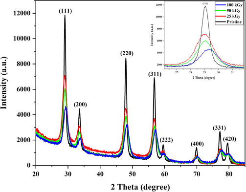
a is an illustration of the XRD patterns for the nanocrystalline CeO2 thin films before (black solid line) and after irradiation with different radiation doses (25, 50 and 100 kGy) using 60Co source. b is an enlargement of (1 1 1) peaks for all samples.
Where D is the crystalline size, ‘λ’ is the X-ray wavelength, θ is the reflection peak angle in degree and ‘β’ is the full width at half maximum (FWHM) in radian. Inset of Fig. 1 shows that, the FWHM is abruptly increased at 25 kGy comparing to the pristine thin films and then decreased as the gamma dose increased. The increase of gamma exposed dose value might be create nano-structural defects that increased in dislocations density at 25 kGy. Then decreased with increasing the radiation dose value, which induce strain and average crystallites size shown the opposite trend comparing to the dislocation density. Comparable result has been described by A Kozlovskiy et al. (Kozlovskiy et al. 2018) who observed that an increase in the irradiation dose leads to an increase in crystallite size and dislocation density under the influence of gamma irradiation. Lattice constant of CeO2 thin films were estimated by XRD peak using following equation (Nelson and Riley, 1945):
Where ‘d’ is the spacing between the planes, (h, k, l) are the plane indices and ‘a’ is the lattice constant. The computed nanostructure results by XRD are given in Table 1.
Gamma dose (kGy)
Crystallite size D (nm)
Micro-strain ε 10-3
Dislocation density δ 1014
Lattice constant (Å)
Energy band gap (eV)
a
0
48.90
15.37
4.18
0.547
3.34
25
20.57
10.39
23.63
0.543
3.55
50
31.43
12.06
10.12
0.546
3.96
100
42.11
16.81
5.63
0.546
3.42
It can be observed that the (1 1 1) plane takes shift towards the lower angle at 25 kGy and then gradually transferred to larger angle with increasing the gamma dose. Actually, gamma irradiation introduces defects in the crystal structure, which makes the host materials swell. This effect may be used for producing thermo-shrinkable or temperature-induced healing of such defects. Therefore, not only the lattice parameter should change as well as producing the shift of the peak.
3.2 Thin films morphology
The morphology of the CeO2 thin films is an important factor to modify their physical properties such optical transmission, refractive index and energy band gap. So, it is significant to examine the morphology of pristine and gamma exposed thin films. Fig. 2 (a-d) displays the characteristic top view FESEM images of thin films with and without gamma exposure. It can be seen from Fig. 2 (a) that the morphology of pristine sample has a spherical shape with grains size of about 28 nm. It is clear from Fig. 2 (b) that the spherical grain size decreased to 19 nm at 25 kGy and after further increasing in irradiation dose the grain size increased to 35 nm. It can be seen that after gamma radiation, the CeO2 thin film has a compressed, smooth and uniform surface morphology. As a result, the morphological properties of the CeO2 thin films have altered significantly by gamma exposed dose.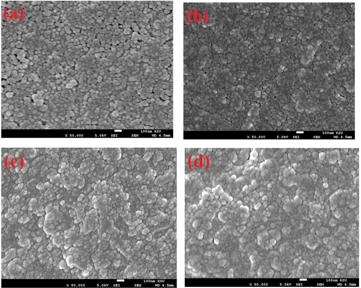
FESEM images of (a) as deposited, (b) 25 kGy, (c) 50 kGy and (d) 100 kGy gamma irradiated CeO2 thin films.
3.3 EDX analysis
The scanned area/or FESEM images from where EDX statistics were obtained and EDX spectrum of as pristine CeO2 film are presented in Fig. 3 (a,b). The analysis confirmed the existence of Ce and O in the prepared films. The atomic ratio of Ce and O almost remain same with increasing gamma exposed dose. The elemental compositions of all samples are given inset of Fig. 3 (b).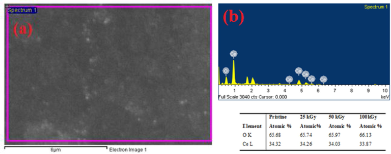
EDX spectra of pristine and gamma irradiated CeO2 thin films.
3.4 UV–Vis spectroscopy
The transmittance spectra of pristine and gamma irradiated CeO2 thin films in the wavelength range of 300–800 nm are shown in Fig. 4 (a). It can be seen that the transmittance decreases to zero in the UV range and increases in the visible region for all samples. The maximum transmittance pristine CeO2 thin films is 69%. After irradiating the CeO2 sample by 25 kGy of gamma ray emitted from 60Co source, the transmittance reaches the 82%. With further increase in gamma irradiation doses, the transmittance decreases and the lowest value was found to be 75% for the case of 100 kGy. The absorption edge first moves to higher energy at 25 kGy and then change to lower energy value with further rise in the gamma dose. The energy bandgap values are calculated by extrapolating the linear portion of the Tauc’s plot ((αhν)2 Vs (hν)) of the pristine and gamma exposed thin films as shown in Fig. 4 (b). The deviation of absorption coefficient (α) with hν was estimated using the following equations: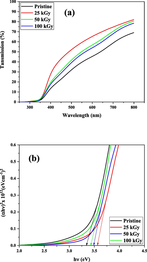
(a) Transmittance spectra (b) Tauc’s plot of pristine and gamma irradiated thin films.
3.5 Photoluminescence properties
Photoluminescence (PL) is a powerful technique to analyze light emission properties of nanostructure thin films. To obtain a deeper understanding of gamma irradiation effects within the CeO2 thin films and its optical response, PL spectra have been measured at room temperature with an excitation wavelength of 325 nm in order to make the PL spectra comparable. Fig. 5 displays the comparison of PL results of pristine and gamma exposed CeO2 thin films. It can be seen that the emission peak in the PL spectra positioned at 408 nm is associated to the intrinsic fluorescence of CeO2 thin films (Babitha et al. 2015). In CeO2, the defect states are existing near the Ce 4f level. Thus bands seemed in the range of 415–500 nm is proposed structural defects attributed with oxygen deficiency in CeO2 thin films (Wang et al. 2011). Thus the emission peaks that appear can be attributed to the oxygen related defects. This band may be ascribed on the base of transition of electron from the 4f conduction band to O 2p valence band the valence of CeO2 thin films. Hence the PL peak created by excited electron–hole recombination, it means higher intensity would suggest a greater recombination rate, representing that pristine CeO2 provide the fastest recombination. However, the intensity of peaks gradually decreased with increasing gamma exposed dose, proposing that the gamma dose decreased recombination rate of the charge carriers.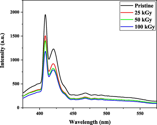
PL spectra of pristine and gamma irradiated CeO2 thin films.
3.6 Hall measurements
To investigate the effect of gamma exposure on electrical characterization of CeO2 thin films, Hall measurement was used to estimate the mobility, electrical resistivity and carrier concentration. Fig. 6 represent the behavior of electrical parameters against the gamma rays exposed dose. It can be seen that the resistivity decreases to its maximum value at 50 kGy and then increases with increasing gamma exposed dose. On the other hand, the carrier concentration has a reverse trend to the resistivity. The mobility is increased up to 25 kGy and then slightly reduced for higher gamma irradiation dose. However, the electrical properties of gamma irradiation thin films are enriched comparing to the pristine CeO2 thin films. The increase of carrier concentration is due to the increase of oxygen deficiency and broken bonds (Baydogan et al. 2013). The mobility generally depends on scattering phenomena like grain boundary scattering and ionized scattering due to irradiation (Lu et al. 2006). The same behavior was obtained by Baydogan et al. reported that the irradiation dose was an important parameter to reduce the electrical resistivity and to increase carrier concentration and mobility of nanostructure ZnO:Al thin film (Baydogan et al. 2013). We can assume from results that the electrical properties of gamma irradiated thin films were improved after exposure.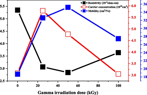
Variation of electrical parameters with gamma irradiated dose of CeO2 thin films.
4 Conclusion
The present research work demonstrates the deposition of CeO2 on glass substrates by spin coating technique. The results mainly described the effects of gamma exposure on nanostructure, morphological, optical and electrical characterization of the prepared thin films. The XRD analysis showed that the intensity decreased for all reflection with increasing the gamma exposed dose value, which indicates that the crystallinity of the CeO2 reduced after gamma exposure. FESEM showed that the grains decreased from with average diameter of ∼ 28 to ∼ 19 nm at 25 kGy, then increased to ∼ 35 nm for further increased in gamma doses. The alteration in morphology associated with the energy transferred to the thin films that created a heating effect in lattice of the CeO2 thin films. The Eg of pristine and gamma exposed film presented the blue shift from 3.34 to 3.55 eV with exposed dose from 0 to 25 kGy and then moved to 3.42 eV as the dose increased to100 kGy. The change in the Eg due to the defects generation or annihilation by irradiation, which generated charge carrier traps inside the band gap. The intensity of PL peaks gradually decreased with an increase in gamma rays exposed dose, proposing that the gamma dose decreased recombination rate of the charge carriers. The PL peak shifting and alteration in with gamma exposure may be due to the lattice divergence of the nanostructure. The electrical characterization of gamma exposure thin films is enriched as compare to the pristine CeO2 thin films. The increase of carrier concentration is due to the increase of density of the defects. The mobility generally depends on scattering phenomena like grain boundary scattering and ionized scattering due to irradiation. Thus, the results of all the above investigation confirm that the CeO2 can be a strong and a good candidate for being used as radiation dosimeter.
Acknowledgements
The authors would like to extend their sincere appreciation to the Deanship of Scientific Research at King Saud University for funding under Research Group No. RG-1441–315.
Declaration of Competing Interest
The authors declare that they have no known competing financial interests or personal relationships that could have appeared to influence the work reported in this paper.
References
- CO2 responses based on pure and doped CeO2 nano-pellets. J. Mater. Res. Technol.. 2018;7:14-20.
- [CrossRef] [Google Scholar]
- Ali, S. M., Ramaya, S. M., Rehman, N. U., ALKhuraiji, T. S., Shar, M. A., Mahmood, A., Hassan, A., Riaz, M., 2019. Investigation of gamma irradiation effects on the properties of CdS/p-Si heterostructure. Materials Science in Semiconductor Processing. 93, 44–49. https://doi.org/10.1016/j.mssp.2018.12.028.
- Structural characterization and optical studies of CeO2 nanoparticles synthesized by chemical precipitation. Indian J. Pure Appl. Phys.. 2015;53:596.
- [Google Scholar]
- The improvement in the electrical properties of nanospherical ZnO: Al thin film exposed to irradiation using a Co-60 radioisotope. Radiat. Phys. Chem.. 2013;89:20-27.
- [CrossRef] [Google Scholar]
- Structure, microstructure and optical properties of cerium oxide thin films prepared by electron beam evaporation assisted with ion beams. Solid State Sci.. 2009;11:1456-1464.
- [CrossRef] [Google Scholar]
- An investigation on palladium sulphide (PdS) thin films as a photovoltaic material. Thin solid film.. 2007;515:5783-5786.
- [CrossRef] [Google Scholar]
- Effect of swift heavy ions irradiation on AlN ceramics propertiesCeramics. International. 2018;44:19787-19793.
- [CrossRef] [Google Scholar]
- Humidity sensing properties of CeO2–NiO nanocomposite materials. J Mater Sci: Mater Electron.. 2015;26:3083-3089.
- [CrossRef] [Google Scholar]
- A highly sensitive γ- radiation dosimeter based on the CeO2 nanowires. Physica E. 2009;41:1550-1553.
- [CrossRef] [Google Scholar]
- Lu, J.G., Ye, Z.Z., Zeng, Y.J., Zhu, L.P., Wang, L., Yuan, J., Zhao, B.H., Liang, Q.L., 2006. Structural, optical and electrical properties of (Zn, Al)O films over a wide range of compositions, J. Appl. Phys., 100, 073714 (1–11). https://doi.org/10.1063/1.2357638
- Radiation sustenance of HfO2/β-Ga2O3 metal-oxide-semiconductor capacitors: gamma irradiation study. Semicond. Sci. Technol.. 2020;35:055024
- [CrossRef] [Google Scholar]
- Effects of ion irradiation on the structural and electrical properties of HfO2/SiON/Si p-metal oxide semiconductor capacitors. Thin Solid Films. 2019;682:156-162.
- [CrossRef] [Google Scholar]
- Enhancement of photosensitivity in chemically deposited CdSe thin films by air annealing. J. Appl. Phys.. 1993;74(3):1879.
- [CrossRef] [Google Scholar]
- An experimental investigation of extrapolation methods in the derivation of accurate unit-cell dimensions of crystals. Proc. Phys. Soc. (London). 1945;57:160.
- [CrossRef] [Google Scholar]
- Pacchioni G., Skuja L., Griscom D.L., eds. Defects in SiO2 and Related Dielectrics: Science and Technology. Dordrecht: Springer Netherlands; 2000.
- Effect of gamma radiation on morphological & optical properties of ZnO nanopowder. Results Phys.. 2017;7:807-809.
- [CrossRef] [Google Scholar]
- Metal Oxide Nanostructures and Their Gas Sensing Properties. Sensors.. 2012;12:2610-2631.
- [CrossRef] [Google Scholar]
- Optical band gap as parameter in gamma rays dosimetry (high doses) Romanian Reports in Physics. 2020;72:803.
- [Google Scholar]
- Role of sodium in radiation defect formation in CsI crystals. Radiat. Meas.. 2001;33:687-692.
- [CrossRef] [Google Scholar]
- Electrochemical deposition of Eu3+-doped CeO2 nanobelts with enhanced optical properties. J. Phys. Chem. C.. 2011;115:351-356.
- [CrossRef] [Google Scholar]
- Toluene degradation over Mn-TiO2/CeO2 composite catalyst under vacuum ultraviolet (VUV) irradiation. Chem. Eng. Sci.. 2019;195:985-994.
- [CrossRef] [Google Scholar]
- Anchoring ceria nanoparticles on graphene oxide and their radical scavenge properties under gamma irradiation environment. Phys. Chem. Chem. Phys.. 2017;19:16785.
- [CrossRef] [Google Scholar]
- Radiation damage in scintillating crystals. Nucl. Instrum. Methods Phys. Res., Sect. A. 1998;413:297-311.
- [CrossRef] [Google Scholar]
- Evaluation of synergistic effects of the single walled carbon nanotube and CeO2-hybrid based-nanocomposite against X-ray radiation in diagnostic radiology. Radiat. Phys. Chem.. 2020;168:108562
- [CrossRef] [Google Scholar]