Translate this page into:
ALD grown nanostructured ZnO thin films: Effect of substrate temperature on thickness and energy band gap
⁎Corresponding authors. asim.jilane@gmail.com (Asim Jilani)
-
Received: ,
Accepted: ,
This article was originally published by Elsevier and was migrated to Scientific Scholar after the change of Publisher.
Peer review under responsibility of King Saud University.
Abstract
Nanostructured ZnO thin films with high transparency have been grown on glass substrate by atomic layer deposition at various temperatures ranging from 100 °C to 300 °C. Efforts have been made to observe the effect of substrate temperature on the thickness of the deposited thin films and its consequences on the energy band gap. A remarkably high growth rate of 0.56 nm per cycle at a substrate temperature of 200 °C for ZnO thin films have been achieved. This is the maximum growth rate for ALD deposited ZnO thin films ever reported so far to the best of our knowledge. The studies of field emission scanning electron microscopy and X-ray diffractometry patterns confirm the deposition of uniform and high quality nanosturtured ZnO thin films which have a polycrystalline nature with preferential orientation along (1 0 0) plane. The thickness of the films deposited at different substrate temperatures was measured by ellipsometry and surface profiling system while the UV–visible and photoluminescence spectroscopy studies have been used to evaluate the optical properties of the respective thin films. It has been observed that the thickness of the thin film depends on the substrate temperatures which ultimately affect the optical and structural parameters of the thin films.
Keywords
Thin films
ALD
Scanning electron microscopy
X-ray diffraction
Optical properties
1 Introduction
Zinc oxide (ZnO) is known to be as n-type semiconductor and a transparent conductive oxide with excellent optoelectronic properties like wide band gap (3.37 eV), high dielectric constant, high exciton binding energy (60 meV), and high thermal stability (Özgür et al., 2005). Hence, it is used in a wide range of applications such as solar cells, gas sensors, optoelectronic devices, biosensors and transducers (Klingshrin, 2007; Look et al., 1999; Pearton et al., 2003; Reynolds et al., 1996; Wraback et al., 1999). ZnO thin films have been prepared by many methods such as RF-magnetron sputtering (Krupanidhi and Sayer, 1984), ion beam-assisted reactive deposition (IBAD) (Zhang and Brodie, 1994), chemical vapor deposition (CVD) (Minegishi et al., 1997), pulsed laser deposition (PLD) (Ryu et al., 2000), molecular beam epitaxy (MBE) (Kang et al., 1998; Segawa et al., 1997) and atomic layer deposition (ALD) (Guziewicz et al., 2008; Keun Kim et al., 2005; Lim et al., 2004). ALD method is a special modification of chemical vapor deposition for self-limiting film growth. It can be considered as one of the best techniques to synthesize nanostructured thin films of the order of few angstroms (Keun Kim et al., 2005; Lim and Lee, 2007; Lim et al., 2004). ALD reactions use two chemicals, typically called precursors which react with the surface of a material one at a time in a sequential, self-limiting manner. When the precursors are exposed to the substrate surface repeatedly, a fine quality ultra-thin film is deposited. Slow deposition growth rates of ALD facilitate several processes as an advantage to ensure uniform high quality and pinhole defect free films over large areas. ALD grown ZnO thin films have gained substantial interest in the field of semiconductor research because of their high purity, ultra thinness and crystallinity which influence the optical and electrical properties of the film and make it a suitable candidate for optoelectronics applications. The optoelectronic devices require optical coating of high quality (good surface uniformity, high packing density, good adhesion with underlying substrate, low defect density) and precise thickness control which depends on the deposition method being used (Martinu et al., 2014).
The structural and optical properties are greatly influenced by the substrate temperature of the thin film, however, there have been few research articles on the substrate temperature dependent thickness and the associated changes in the structural, optical and electrical properties of the ZnO thin films (Ahmad et al., 2015). These physical properties of ZnO thin films are affected by the mechanism and growth conditions such as substrate temperature, pressure, precursors and thickness (Enigochitra et al., 2015). For optoelectronic devices based on ZnO thin films, influence of a parameter such as substrate temperature on the structural and optical properties is of great importance (Rahal et al., 2014). This work aims to achieve maximum growth rate of ZnO thin films deposited by ALD at different substrate temperatures and the associated changes on the thickness and energy band gap.
1.1 Experimental setup
In our present study we have used Syskey Atomic Layer Deposition system for the deposition of ultra-thin ZnO layers. Diethyl zinc, Zn(C2H5)2 precursor and water as an oxidant have been used in this experiment. Before the deposition of thin films, the substrate (glass slides) was cleaned in an ultrasonic bath with solvents (trichloroethylene, acetone and isopropanol) and finally with deionized water. ALD reaction mechanism for ZnO thin films cycle may be summarized in a single equation:
Cyclic repetition of the above process results into layer by layer growth of ZnO thin films at atomic scale. In all experiments both precursors were kept at room temperature 22–24 °C in the lab, while a substrate temperature was increased from 100 °C to 300 °C with an interval of 50 °C. During all experiments the water (H2O) pulsing time was kept constant at 15 ms, DEZ pulsing time 60 ms and purging flow time 10,000 ms. We achieved the maximum growth of ZnO thin films at a substrate temperature of 200 °C i.e., 0.56 nm per cycle which is evident to be the best deposition rate using ALD ever reported in the literature (Chaaya et al., 2013; Lim et al., 2004; Singh et al., 2014).
1.2 Thin film characterization
Different physical properties of the deposited ZnO thin films have been characterized by several techniques. The surface characterization have been performed by field emission scanning electron microscopy (FESEM-JSM7600F JEOL – Japan), while the XRD (Ultima-IV; Rigaku, Japan) patterns gave the crystalline structure and phases of grown ZnO thin films. Ellipsometry (Horiba UVISEL, France) and surface profiler (Dektak, Bruker-Germany) have been used for thickness measurements of the thin films. Finally the UV–visible spectrometer (Perkin Elmer Lambda 750) and photoluminescence (PL) spectrometer (RF-5301PC-Shimadzu, Japan) devices have been used to investigate the optical properties of the thin films.
2 Results and discussion
2.1 Surface characterization
Surface morphology studies of thin films have been conducted using FESEM. Fig. 1 shows the FESEM images of ZnO thin films at a high resolution. It has been observed that the particle size of ZnO thin films increases with the increase in temperature up to 200 °C and decreases when the temperature was increased further from 200 °C to 300 °C. These changes in the particle size at different substrate temperatures show the effect of temperature on growth mechanism of the thin film. The decrease in the energy band gap (Eg) with the increase in the films thickness is due to the increase in localized density of states near the band edges which results in the decrease in Eg with thickness. The decrease in direct Eg with the increase in film thickness can also be associated with an increase in particle size (Seval et al., 2010). This shows the dependence of Eg on the thin film thickness. These results are also in good agreement with the literature (Alnajjar, 2012).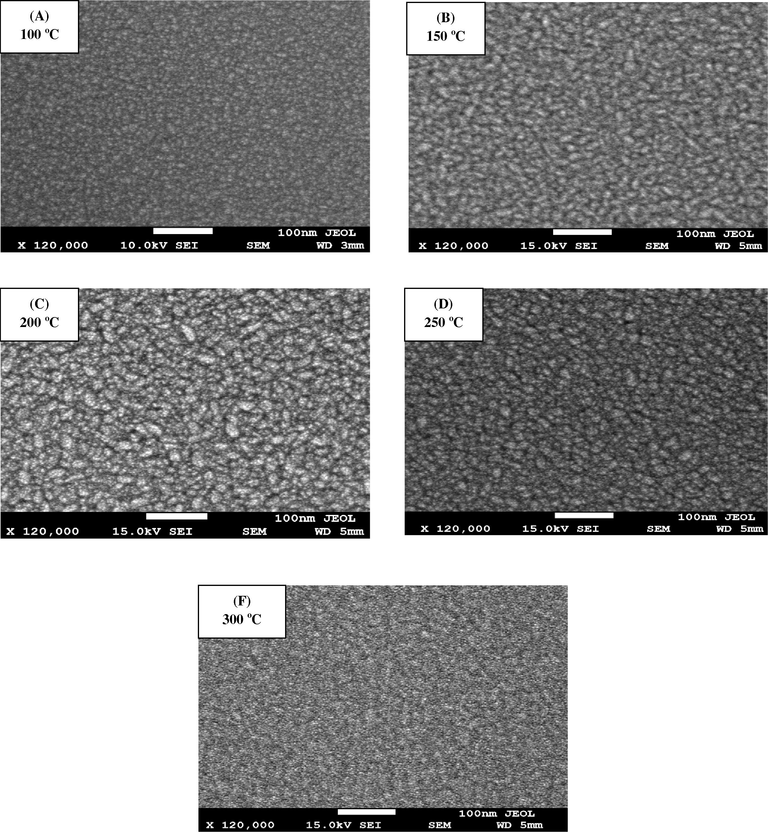
FESEM micrograph of ZnO thin films deposited at different substrate temperatures (A) 100 °C (B) 150 °C (C) 200 °C (D) 250 °C (E) 300 °C. All the images were taken at 120 k magnification with SEI detector and the scale shown is 100 nm in size.
2.2 Thickness measurement
The thickness of the films has been measured by ellipsometry (Horiba UVSEL, France). We observed 14.1 nm, 27.6 nm, 33.4 nm, 30.7 nm and 23.07 nm thicknesses for 100 °C, 150 °C, 200 °C, 250 °C and 300 °C substrate temperatures respectively. These results were also confirmed with the surface profiling system (Dektak Bruker, Germany).
2.3 Structural characterization
For the structural analysis of ZnO nanostructured thin films, we have used X-ray diffraction (XRD) measurements. The analysis was performed using Ultima-IV Rigaku XRD system with Cu-Kα radiation (λ = 1.54060 nm) operated at 40 kV and 40 mA at room temperature. The XRD spectra were measured in the 2θ angular region between 25° and 75°. The XRD patterns of thin films obtained at different substrate temperatures are shown in Fig. 2. All the patterns clearly reveal the polycrystalline structure with orientation along different planes. These planes are (1 0 0), (0 0 2), (1 0 1), (1 0 2), (1 1 0), (1 0 3) and (1 1 2) of ZnO nano structures, indicating that the samples are polycrystalline wurtzite structure (Zincite, ICDD-PDF card No. 01-074-9940). The 4-index notation of all XRD patters is shown below in Table 1. The XRD patterns consists of the major diffraction peak of ZnO at an angle (2θ) of 32.1° along (1 0 0) plane while the others with low intense peaks attributed to (0 0 2), (1 0 1), (1 0 2), (1 1 0), (1 0 3) and (1 1 2) planes. It is clear from the XRD patterns that the initial increase in the temperature from 100 °C to 200 °C results in improved crystallinity along (1 0 0) as the major peak intensity considerably increases up to 200 °C. Afterward the major peak intensity of the thin film decreases above 200 °C substrate temperature. The change in the peak intensity is associated with the change in the structural parameters. The Full width at half maximum (FWHM) of ZnO peaks also changes with the change in the substrate temperature. This indicates that the growth, orientation and grain size of ZnO nanocryatals depend on the substrate temperature. The following Debye Scherrer formula (Gordillo et al., 1995) has been used to calculate the grain size of the deposited thin films
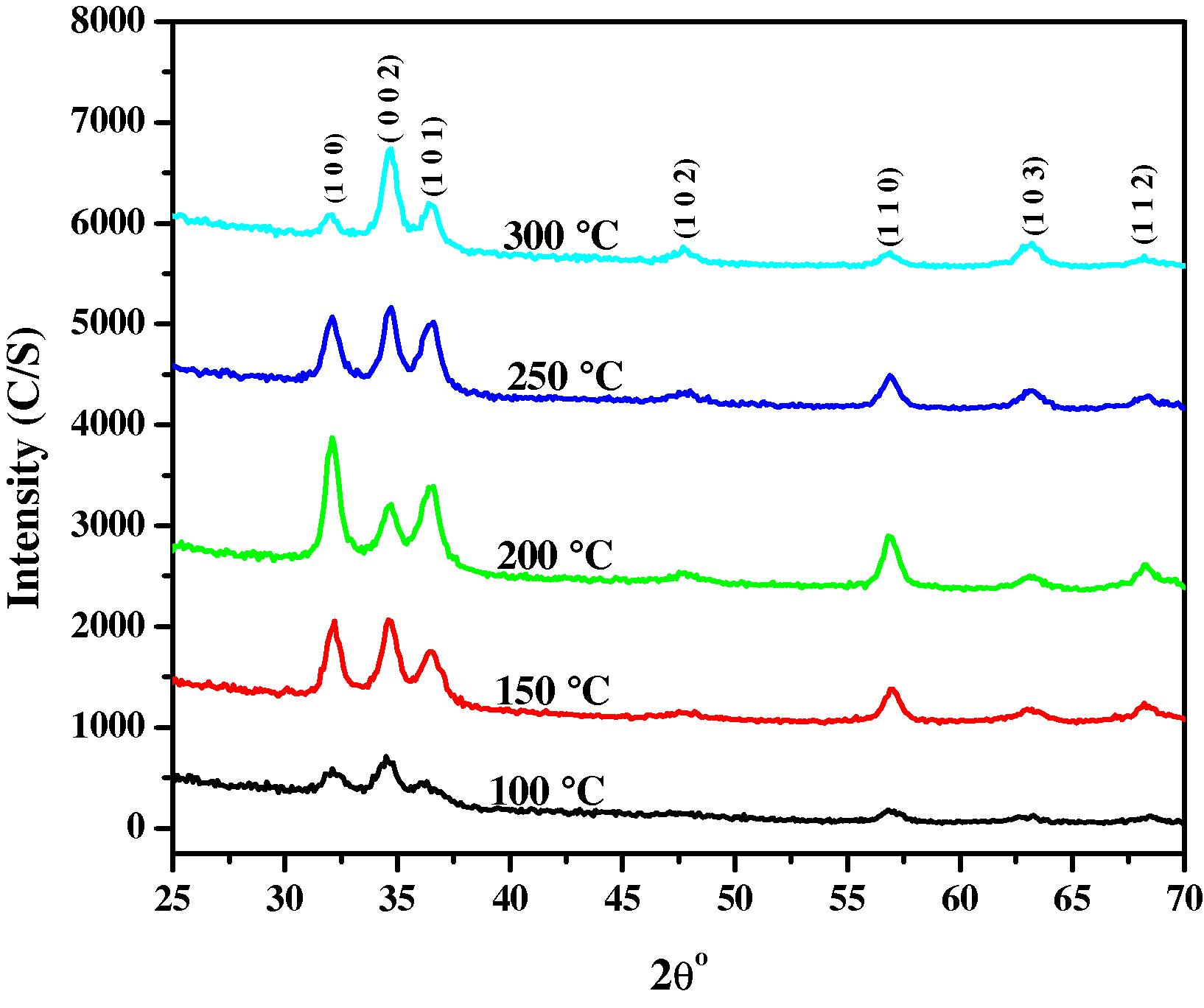
XRD patterns of ZnO thin films deposited at different substrate temperatures.
Peak position at 2θ (°)
(h k l)
(h k i l)
31.1
(1 0 0)
(1 0
0)
34.7
(0 0 2)
(0 0 0 2)
36.4
(1 0 1)
(1 0
1)
47.9
(1 0 2)
(1 0
2)
56.9
(1 1 0)
(1 1
0)
62.8
(1 0 3)
(1 0
3)
68.1
(1 1 2)
(1 1
2)
The above relation verifies that if the crystallite size increases then dislocation density decreases. Since, the dislocation density and strain are the manifestations of dislocation network in the films, the decrease in the strain and dislocation density indicates the formation of higher quality films (Lalitha et al., 2004).
2.4 Optical characterization
UV–visible spectrophotometry (Perkin Elmer Lambda 750) was used to obtain the wave length (λ) dependent transmission (T) and absorbance (A) spectra. Data acquisition was made at room temperature. Fig. 3(A) and (B) shows the overlap graph of optical absorbance and transmission spectra respectively, obtained for the five ZnO thin films grown at different substrate temperatures ranging from 100 °C to 300 °C with an interval of 50 °C. It can be noticed that the absorbance of thin films, in Fig. 3(A), increases with the increase in the substrate temperature up to 200 °C and then starts decreasing as the substrate temperature was increased further from 200 °C to 300 °C. These changes in the absorbance are associated with the film thicknesses which have been deposited at different substrate temperatures. An increase in the absorbance is due to increase in the thin film thickness which may increase in the carrier concentration which blocks the energy. The decrease in the absorbance of the thin films which were deposited at substrate temperatures of 250 °C and 300 °C allowing to pass more energy due to decrease in the thin film thickness.Fig. 3(B) shows the optical transmittance above 89.88% in the visible wavelength range, which complements the absorbance spectra.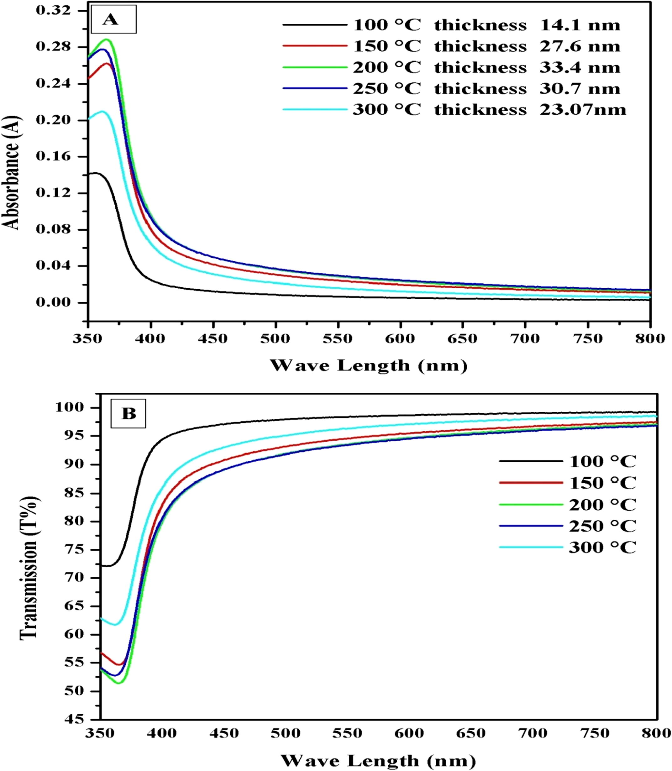
(A and B). UV–visible absorbance and transmittance spectra of the ZnO thin films deposited at different substrate temperatures 100 °C, 150 °C, 200 °C, 250 °C and 300 °C.
The relation between transmittance, T and absorption coefficient, α in the high absorption region is expressed in the following equation:
The energy band gap Eg can be calculated by assuming a direct transition between valence and conduction bands. The absorption coefficient α as a function of photon energy can be expressed as in the following equation (Lalitha et al., 2004):
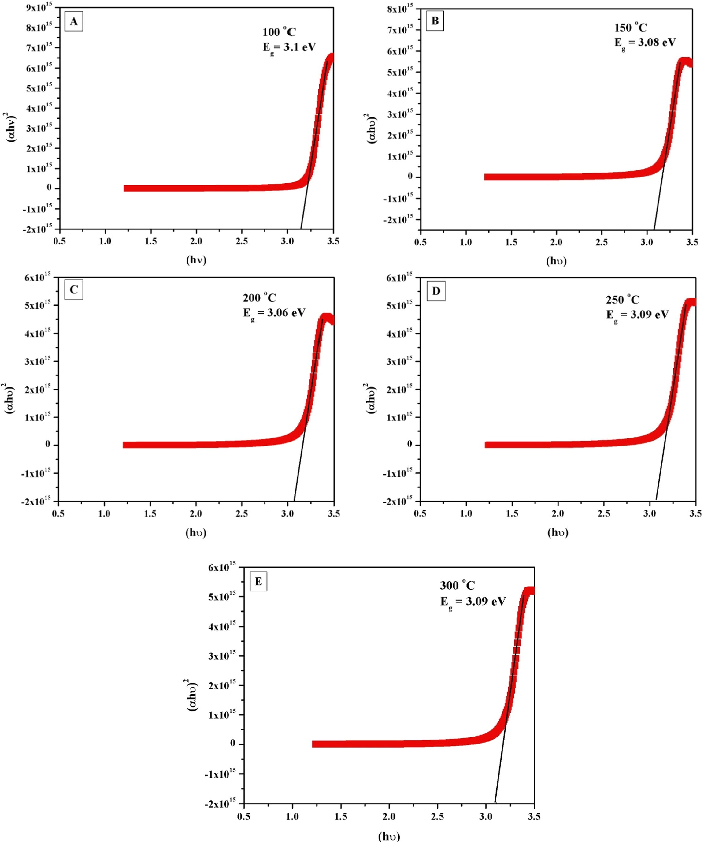
Plot of (αhν)2 versus photon energy, hυ of ZnO thin films deposited at different substrate temperatures 100 °C, 150 °C, 200 °C, 250 °C and 300 °C.
Substrate temperature (°C)
100
150
200
250
300
ZnO thin film thickness (nm)
14.1 ± 0.03
27.6 ± 0.60
33.4 ± 0.50
30.7 ± 0.75
23.07 ± 0.66
Growth rate (nm/cycle)
0.24
0.46
0.56
0.51
0.38
Energy band gap (eV)
3.10
3.08
3.06
3.07
3.09
Refractive index (n)
1.52
1.54
1.56
1.55
1.53
Dielectric constant (ε∞)
2.31
2.37
2.44
2.40
2.35
Static dielectric constant (ɛo)
19.18
18.71
17.97
18.34
19.18
The optical properties of semiconductor materials mainly depend on the energy band gap, refractive index and dielectric constant. The applications of semiconductors in electronics, optical and optoelectronic devices are very much determined by the magnitude of these elementary properties of the materials. The refractive index of the films was calculated using Moss Relation (Gupta and Ravindra, 1980; Hannachi and Bouarissa, 2009) which is directly related to the Eg shown in the following expression:
The dielectric constant of solid material is very important for optoelectronics because a change in the energy band gap causes a change in the dielectric constant, which indirectly alters the ionization energies of impurity atoms and the binding energy of the excitons.
The static and high frequency dielectric constants were calculated for thin films. For high frequency dielectric constant (ε∞), we used the following relation (Hannachi and Bouarissa, 2009):
For all ZnO films prepared at different substrate temperatures, the calculated values of Eg, n, ε∞ and ɛo are shown in the following Table 2. It can be noted that we have obtained lower energy band gap reported in the literature, therefore, the associated optical parameter like dielectric constant and refractive index also have lower values for the ALD grown ZnO nano structured thin films.
The photoluminescence spectra of ZnO thin films at different substrate temperatures are shown in Fig. 5. The photoluminescence spectra were obtained at room temperature. It can be noticed that all the prepared ZnO thin films having the strong UV emission which is the indication of good crystallinity and enhanced optical properties of prepared ZnO thin films (Zhang et al., 2009). The shift in the ultra violet emission was found from 391 nm to 393 nm. The peak at 391 nm corresponds to free exciton or bound exciton of ZnO in the UV region while the peak shift toward 393 nm is due to ultra violet emission of ZnO. The UV emission is associated to the near band edge emission of ZnO which may be due to the decay of exciton.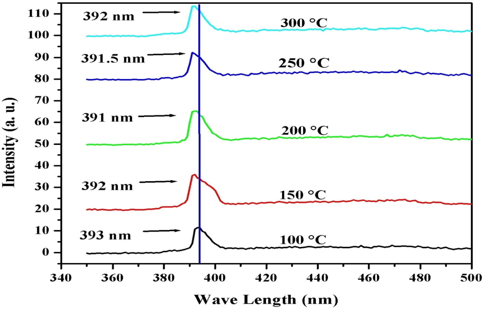
Photoluminescence spectroscopy graphs for ZnO thin films deposited at different substrate temperatures.
3 Conclusion
High purity ZnO thin films of different thickness were deposited by atomic layer deposition through diethyl zinc, Zn (C2H5)2 as a zinc precursor and water as an oxidant. The optimization of ALD growth parameters results in a maximum growth rate of 0.56 nm per cycle. According to our literature survey this is the highest growth rate ever reported. The thin film thickness was found to be varied between 14.1 ± 0.03 nm to 33.4 ± 0.50 nm when the substrate temperature was increased from 100 °C to 300 °C. We have observed the maximum growth of ZnO thin films at 200 °C i.e., 33.4 ± 0.50 nm and the associated refractive index and dielectric constant were found to be 1.56 and 2.44 respectively. The variation in the energy band gap was from 3.06 eV to 3.10 eV with the change in the substrate temperature. A systematic study on the influence of the substrate temperatures on structural and optical properties of ZnO thin films deposited by ALD has been reported.
References
- The effect of substrate temperature on structural and optical properties of D.C. sputtered ZnO thin films. Phys. B Condens. Matter. 2015;470–471:21-32.
- [CrossRef] [Google Scholar]
- ZnO: Al grown by sputtering from two different target sources: a comparison study. Adv. Condens. Matter Phys.. 2012;2012:1-8.
- [CrossRef] [Google Scholar]
- Materials science in semiconductor processing annealing and light effect on optical and electrical properties of ZnS thin films grown with the SILAR method. Mater. Sci. Semicond. Process.. 2007;10:281-286.
- [CrossRef] [Google Scholar]
- Materials Science and Engineering: An Introduction. New York: John Wiley and Sons; 1997.
- Evolution of microstructure and related optical properties of ZnO grown by atomic layer deposition. Beilstein J. Nanotechnol.. 2013;4:690-698.
- [CrossRef] [Google Scholar]
- Influence of substrate temperature on structural and optical properties of ZnO thin films prepared by cost-effective chemical spray pyrolysis technique. Superlattices Microstruct. 2015
- [CrossRef] [Google Scholar]
- Preparation and characterization of CdTe thin films deposited by CSS. Sol. Energy Mater. Sol.. 1995;37:273-281.
- [Google Scholar]
- Extra-low temperature growth of ZnO thin films by atomic layer deposition. J. Korean Phys. Soc.. 2008;53:2880-2883.
- [CrossRef] [Google Scholar]
- Band parameters for cadmium and zinc chalcogenide compounds. Phys. B Condens. Matter. 2009;404:3650-3654.
- [CrossRef] [Google Scholar]
- Epitaxial growth of ZnO films on (0 0 0 1) sapphire at low temperatures by electron cyclotron resonance-assisted molecular beam epitaxy and their microstructural characterizations. Jpn J. Appl. Phys. Part 1 Regul. Pap. Short Notes Rev. Pap.. 1998;37:781-785.
- [CrossRef] [Google Scholar]
- Comparison between ZnO films grown by atomic layer deposition using H2O or O3 as oxidant. Thin Solid Films. 2005;478:103-108.
- [CrossRef] [Google Scholar]
- ZnO: from basics towards applications. Phys. Status Solidi. 2007;244:3027-3073.
- [CrossRef] [Google Scholar]
- Position and pressure effects in RF magnetron reactive sputter deposition of piezoelectric zinc oxide. J. Appl. Phys.. 1984;56:3308.
- [CrossRef] [Google Scholar]
- Characterization of CdTe thin film – dependence of structural and optical properties on temperature and thickness. Sol. Energy Mater. Sol. Cells. 2004;82:187-199. 10.1016/j.solmat.2004.01.017
- [Google Scholar]
- Effects of substrate temperature on the microstructure and photoluminescence properties of ZnO thin films prepared by atomic layer deposition. Thin Solid Films. 2007;515:3335-3338.
- [CrossRef] [Google Scholar]
- Photoluminescence studies of ZnO thin films grown by atomic layer epitaxy. J. Lumin.. 2004;109:181-185.
- [CrossRef] [Google Scholar]
- Production and annealing of electron irradiation damage in ZnO. Appl. Phys. Lett.. 1999;75:811.
- [CrossRef] [Google Scholar]
- Advances in optical coatings stimulated by the development of deposition techniques and the control of ion bombardment. SVC Bull. 2014:36-45.
- [Google Scholar]
- Growth of p-type zinc oxide films by chemical vapor deposition. Jpn. J. Appl. Phys.. 1997;36:1453-1455.
- [CrossRef] [Google Scholar]
- Influence of thickness and substrate temperature on electrical and photoelectrical properties of vacuum-deposited CdSe thin films. Mater. Chem. Phys.. 2002;78:51-58.
- [Google Scholar]
- Recent progress in processing and properties of ZnO. Superlattices Microstruct.. 2003;34:3-32.
- [CrossRef] [Google Scholar]
- Substrate temperature effect on optical property of ZnO thin films. Eng. J.. 2014;18:81-88.
- [CrossRef] [Google Scholar]
- Energy gap-refractive index relations in semiconductors – an overview. Infrared Phys. Technol.. 2007;50:21-29.
- [CrossRef] [Google Scholar]
- Effect of film thickness on the structural morphological and optical properties of nanocrystalline ZnO films formed by RF magnetron sputtering. Adv. Mater. Lett.. 2012;3:239-245.
- [CrossRef] [Google Scholar]
- Optically pumped ultraviolet lasing from ZnO. Solid State Commun.. 1996;99:873-875.
- [CrossRef] [Google Scholar]
- Optical and structural properties of ZnO films deposited on GaAs by pulsed laser deposition. J. Appl. Phys.. 2000;88:201-205.
- [CrossRef] [Google Scholar]
- Growth of ZnO thin film by laser MBE: lasing of exciton at room temperature. Phys. Status Solidi. 1997;202:669-672. doi:10.1002/1521-3951(199708)202:2<669::aid-pssb669>3.0.co;2-t
- [Google Scholar]
- Effect of Sn dopants on the optical and electrical properties of ZnO films. Opt. Appl.. 2010;XL:9-14.
- [Google Scholar]
- Thickness dependence of optoelectronic properties in ALD grown ZnO thin films. Appl. Surf. Sci.. 2014;289:27-32.
- [CrossRef] [Google Scholar]
- Dependence of film thickness on the structural and optical properties of ZnO thin films. Appl. Surf. Sci.. 2009;255:6195-6200.
- [CrossRef] [Google Scholar]
- High contrast, ultrafast optically addressed ultraviolet light modulator based upon optical anisotropy in ZnO films grown on R-plane sapphire. Appl. Phys. Lett.. 1999;74:507.
- [CrossRef] [Google Scholar]
- Studies on cadmium selenide (CdSe) thin films deposited by spray pyrolysis. Mater. Chem. Phys.. 2010;121:53-57.
- [CrossRef] [Google Scholar]
- Influence of films thickness and structure on the photo-response of ZnO films. Opt. Commun.. 2010;283:1370-1377.
- [CrossRef] [Google Scholar]
- Effects of annealing ZnO films prepared by ion-beam-assisted reactive deposition. Thin Solid Films. 1994;238:95-100.
- [CrossRef] [Google Scholar]
- Photoluminescence and Raman scattering of ZnO nanorods. Solid State Sci.. 2009;11:865-869.
- [CrossRef] [Google Scholar]


