

Translate this page into:
Enhanced optical transmittance of silver nanowires via gamma rays irradiation
⁎Corresponding author at: Department of Physics, University of Okara, Okara, Pakistan. shehlahoney@yahoo.com (Shehla Honey)
-
Received: ,
Accepted: ,
This article was originally published by Elsevier and was migrated to Scientific Scholar after the change of Publisher.
Peer review under responsibility of King Saud University.
Abstract
Metallic nanowires (MNWs) are of particular interest as transparent electrodes (TEs) in optoelectronic devices due to their outstanding and unique optical, electrical and mechanical capabilities. In present research, we systematically studied the influence of gamma radiations (γ-radiations) on silver nanowires (AgNWs). We irradiated AgNWs with various doses of γ-radiations ranging between 12 kGy and 20 kGy. After irradiation, we studied the structural properties of un-irradiated and γ-irradiated AgNWs via X-ray diffraction (XRD). The XRD analysis of un-irradiated sample confirmed the pure crystalline metallic nature of un-irradiated AgNWs with crystallite size 29.80 nm. The XRD analysis of irradiated samples revealed the face centered cubic (FCC) crystalline structure at all doses of γ-radiations. The crystallite sizes have been observed to be 31.99 nm, 33.94 nm and 32.56 nm for samples irradiated by γ-radiations of doses 12 kGy, 15 kGy and 20 kGy respectively. XRD data was also used to investigate structural factors such as dislocation density and strain in material. Morphological studies were carried out via transmission electron microscopy (TEM). The TEM images revealed that silver nanoparticles (AgNPs) are formed on outer surfaces of AgNWs after γ-irradiation. After γ-irradiation, optical transmittances have been enhanced up to dose 15 kGy which is might be due to formation of NPs on Ag-NWs.
Keywords
Silver nanowires
Gamma rays
Irradiation
TEM
XRD
UV–VIS

1 Introduction
Transparent electrodes (TEs) are notably used as key parts in lots of optoelectronic device consisting of light emitting diodes (LEDs), power presentations and photovoltaic cells. Their particular aggregate of excessive electric conductivity and optical illumination provides a possibility to behavior strength even as transmitting light through a layer (Groep et al., 2012).
Within the current industry of TEs production, Indium Tin Oxides (ITOs) are regularly utilized in a diffusion of applications but withstand a wide variety of massive discounts, which include high material expenses, (Groep et al., 2012; Kuang et al., 2011) indium deficiency, damage to dwelling substrates at some stage in spraying (Groep et al., 2012); and brittleness (Groep et al., 2012; Catrysse and Fan, 2010; Kuang et al., 2011). To put back the visible electrodes based totally on ITOs, a diffusion of special nanomaterials are advanced like carbon nanotube (CNTs) networks, (Hecht et al., 2011) graphene based thin films, metallic grids and MNWs networks (Hecht et al., 2011; Kumar and Zhou, 2010; Hu et al., 2011; Ellmer, 2012). Amongst these materials, MNWs such as AgNWs are the primary engineers of such electrode based on networks because of ease of synthesis, high aspect ratio, physical properties and mechanical flexibility (Catrysse and Fan, 2010). AgNWs networks can be without difficulty randomly deposited through a number of financial solution-processing techniques such as spray coating (Tenent et al., 2009; Lu and Chou, 2010; Scardaci et al., 2011; Kim et al., 2013); drop casting (Lee et al., 2010; Hardin et al., 2011), and spin coating (Chung et al., 2012; Leem et al., 2011; Liu and Yu, 2011). All of those methods are easy, inexpensive and do not require a big expensive vacuum gadget. Further, those methods are compatible with various low temperature deposition processes. Amongst those methods, spraying is the most cost effective and may be effortlessly carried out. Thin films made by using means of coatings with a solution sprays are properly matched and have a tendency to produce networks greater uniform (Manikandan et al., 2015; Murmu et al., 2021; Honey et al., 2017). The TEs of thin films processed by means of solutions have already revealed their integration competencies in numerous electrical and optoelectronic devices including photovoltaic cells (Leem et al., 2011). However, managing solutions in colloidal form and making them a thin films often makes it hard to come across high renaissance. Moreover, improvement in optical transparency of nanowires networks remains a challenge to improve the optical performance of TEs.
In the present work, we deposited random meshes of AgNWs on glass substrates and subsequently irradiated by γ-radiations of energy 5 mega electron volt (MeV). We found the appearance of AgNPs on AgNWs after γ-irradiations. Optical transmittances of the irradiated AgNWs meshes were found to be increased which is might be due to formation of these NPs on AgNWs.
2 Experimental techniques
AgNWs bought from Advance Chemicals Supplier (ACS) Material (Product identity: AgNWs-One hundred and twenty). The average AgNWs diameters variety is between a hundred and twenty to two hundreds nanometers (nm). The average length is twenty micrometer (µm). Those had been dissolved in iso-propanol with a concentration of 20 mg/ml diluted to 0.1 mg/ml. This solution was drop casted on a glass substrate placed on a warm plate at 160 °C for rapid evaporation of iso-poropanol. The whole experimental scheme is shown in Fig. 1.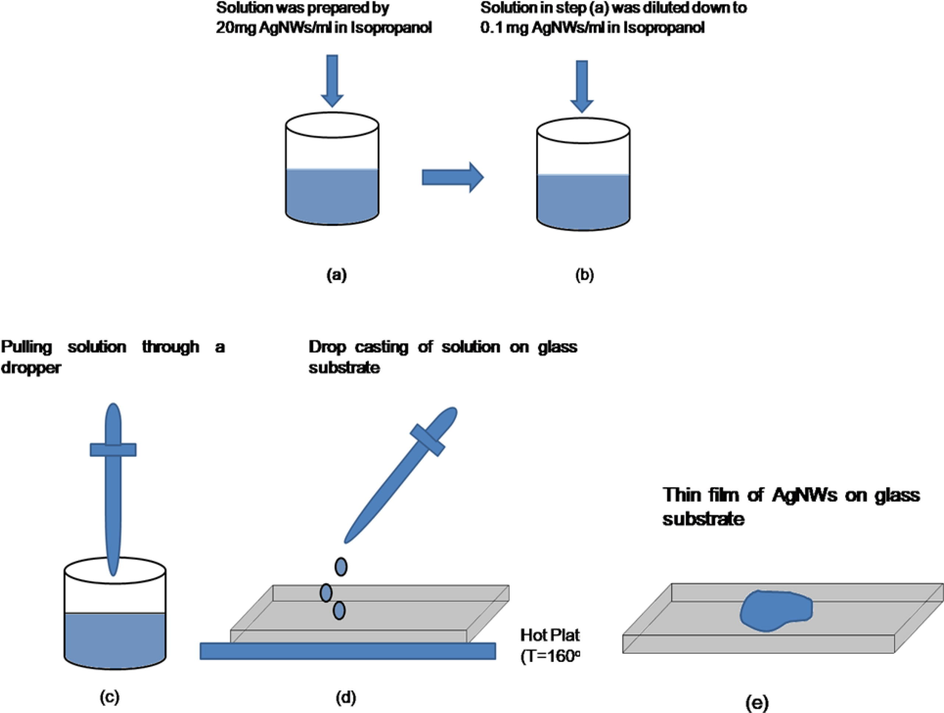
The experimental set up of drop casting of solution of AgNWs on glass substrate.
For structural and optical analysis, the film-coated glass substrate cut into smaller pieces in order to expose to γ-radiations. For analysis of samples by transmission electron microscopy (TEM), solution of AgNWs is dispersed on a copper grids which were placed on glass substrates.
All samples were subsequently exposed to γ-radiations of energy 5 mega electron volt (MeV) and doses 12, 15, and 20 kGy using the Co60 source at room temperature and under air pressure. Dose rate of γ-source was 38 Gy/min. Exposure time for different doses was calculated from the source function, as shown in Table 1. Samples were characterized using multiple techniques such as high resolution transmission electron microscopy (HRTEM), EDX, and X-ray diffraction (XRD). Structural studies of un-irradiated and γ-irradiated samples of various radiation doses, i.e., 12–20 kGy were investigated with XRD data. XRD data were collected at 2θ angular range from 30° to 60° during the installation of 2 s in 0.02 steps using a Bruker X-ray diffractometer with CuKα radiation (1.5409Ao). Optical transmittance was detected using UV–Vis spectroscopy.
Dose (kGy)
Exposure Time
12
5 h 16 min 18 s
15
6 h 35 min 13 s
20
8 h 26 min 31 s
3 Results and discussions
The main purpose of XRD is to analyze the structure of AgNWs before and after exposing to γ-radiations. In Fig. 2(a), XRD spectrum of un-irradiated sample is shown. We plotted a graph between 2θ values and intensity.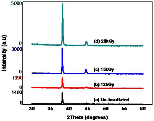
XRD spectra of (a) un-irradiated (b) irradiated at 12 kGy (c) 15 kGy and (d) 20 kGy.
From the Fig. 2(a), the 2θ values ranges between 30° to 60° while the intensity range is between 0 and 1600. There are two different peaks observed on angles 38.230 and 44.690 and we observed from graph that the plane (hkl) values are (1 1 1) and (2 0 0) obtained for un-irradiated AgNWs sample. If the planes of (hkl) values are all even or odd then structure will be face centered cubic (fcc). In this observation, plane values are odd and even so structure of AgNWs is fcc. These peaks represent that material is AgNWs. Moreover, Fig. 2 (a) shows that first peak of (1 1 1) plane having high intensity and also called mean peak and second peak at (2 0 0) plane having low intensity. Fig. 2 (b) shows the XRD spectrum of sample irradiated by γ-radiations of dose 12 kGy. We observed the two different peaks at 38.25° and 44. 69° with (hkl) values (1 1 1) and (2 0 0). Fig. 2(b) shows that the intensity of (1 1 1) peak at 2θ = 38.4° is stronger in contrast to (2 0 0) peak at 2θ = 44.84°. It means that (1 1 1) is preferred position of AgNWs. In this graph, the peak intensity is increasing. But there is no angle shifting observed at this dose. The results are indicating that AgNWs having fcc structure.
Fig. 2(c) shows XRD spectrum after irradiation AgNWs at dose 15 kGy. We observed the two different peaks at angles 38.23° and 44.69° corresponding to planes (1 1 1) and (2 0 0). The intensity of (1 1 1) peak at 2θ = 38.23° is clearly higher than (2 0 0) peak at 2θ = 44.69°. In this graph, the peak intensity is increasing as compared to previous sample.
Fig. 2(d) shows the XRD spectrum of sample irradiated by γ-radiations of dose 20 kGy. The intensity was in the range of 0 to 5000 while value of 2 was in the range of 30 to 60 as for all previous samples. We observed from the graph that there are two peaks present at angle 38.290 44.690 while the hkl values are (1 1 1) and (2 0 0). In this graph, the peak intensity is increased in comparison with previous doses. But there is no angle shifting observed.
We also used XRD data to measure the size of crystal and lattice parameter. There are many factors which effect crystal shape, size and lattice parameter. We use Scherer’s formula to measure the size of crystal.
Fig. 3 shows the graph between dose and average grain sizes for all samples. The doses are 0 kGY,12 kGy, 15 kGy and 20 kGy where 0 kGy is selected to represent un-irradiated sample. 12 kGy, 15 kGy and 20 kGy are doses of irradiated samples. The average grain size of un-irradiated sample is found to be Davg = 29.80 nm. The average grain sizes for samples irradiated at 12 kGy, 15 kGy and 20 kGy are 31.99 nm, 33.94 nm and 32.56 nm respectively.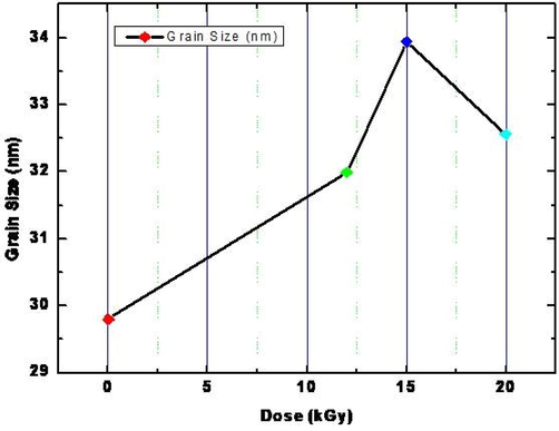
Average grain size of AgNWs before and after irradiation.
In above graph (Fig. 3), it is found that average grain size is increasing after irradiation and as dose was increased from 12 kGy to 15 kGy which is later decreased to 32.56 nm after irradiating the sample by 20 kGy dose of γ-radiations. The reason of reduction in grain size is might be the reduction in crystalline quality of material at this dose.
From XRD data, we determined the strain (τ) of AgNWs at each dose, by using a formula which is given below;
Here is the line that is full width half maximum. is the Bragg’s angle.
After calculating the strain of two peaks of AgNWs at each dose, taking the average of these two values and repeating this process for all four samples, we obtained average strain which is shown in Fig. 4.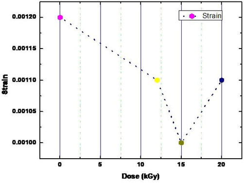
Average strain of AgNWs before and after γ-irradiation.
The graph between dose of γ-radiations and strain (Ʈ) is shown in Fig. 4. The value of strain for un-irradiated sample is Ʈ = 0.0012. After irradiating at 12 kGy, 15 kGy, the values of strain are decreased and found to be Ʈ = 0.0011 and 0.0010 which is then increased slightly to 0.0011 after irradiating sample at 20 kGy.
The existence of strain in the as-prepared and γ-irradiated AgNWs samples is indicated by the deviation of the lattice constant from bulk value. The displacement of atomic locations from their perfect order in nanocrystals causes this difference. The atom rearrangement also causes the nanocrystals' different peaks to expand. When atoms dislocate, the lattice deforms. In crystalline materials, dislocations are imperfections in the lattice.
Eq. (3) was used to calculate the dislocation density in the sample.
The graph between doses and dislocation density is shown in Fig. 5. The dislocation density of un-irradiated sample is found to be Δ = 2.800672 m−2. The dislocation density of samples irradiated by 12 kGy and 15 kGy are decreased and found to be Δ = 2.800305 m−2 and 2.799849 m−2. The dislocation density of sample irradiated at 20 kGy is slightly increased as compared to previous samples and is found to be Δ = 2.800208 m−2. As we observed, the values of strain and dislocation densities are firstly decreased up to dose 15 kGy and then increased at last dose 20 kGy which is might be due to improvement in crystalline quality of films. However, the dislocation density and strain are decreased at last dose which is might be due to production of defects.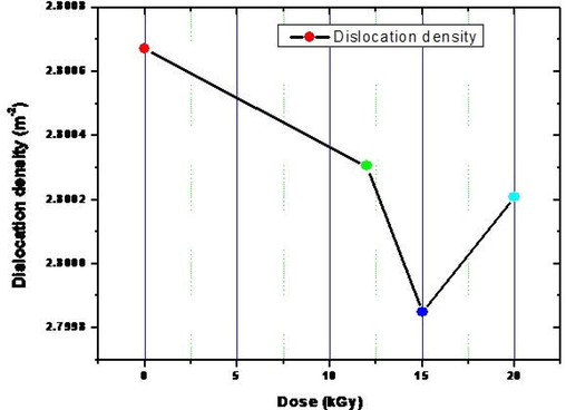
Dislocation density of AgNWs before and after γ-irradiation at various doses.
The shape, size distribution, and crystallographic orientation of nanomaterials are studied using transmission electron microscopy (TEM). On the other hand, crystalline analysis of AgNWs was performed by high resolution transmission electron microscopy (HRTEM). Fig. 6(a) shows TEM image of un-irradiated AgNWs. Fig. 6 (b) shows HRTEM image of AgNWs before irradiation. This shows that nanowires are polycrystalline in nature. The polycrystallinity of AgNWs is further confirmed through selected area electron diffraction (SAED) during TEM analysis. SAED pattern is shown in Fig. 6 (c). SAED pattern shows that structure of un-irradiated AgNWs is polycrystalline before irradiation. During TEM, energy dispersive X-ray spectroscopy (EDX) was used to determine the chemical composition of AgNWs as shown in Fig. 6 (d). The EDX spectrum consists of the elements Ag, C, Cu, and O. The Ag peak came from the AgNWs, the C and Cu peaks came from the carbon which was coated during TEM and Cu is due to Cu gird on which sample was prepared. Oxygen peak might be appeared due to oxidation of Cu grid.
Un-irradiated AgNWs (a) TEM image (b) HRTEM image (c) SAED pattern (d) EDX spectrum.
After irradiating Ag-NWs by gamma rays of dose 12 kGy, the nanoparticles appeared on outer surface of Ag-NWs and can be seen in Fig. 7. These Nanoparticles are may be formed due to gamma rays induced sputtering of atoms from Ag-NWs which were then accumulated on the surface and grow in form of nanoparticles on the surfaces of AgNWs. Sputtering may be happened due to γ-radiations induced collision cascade effect which finally ejected the atoms from the lattice and accumulate these atoms on the surfaces of NWs in form of NPs.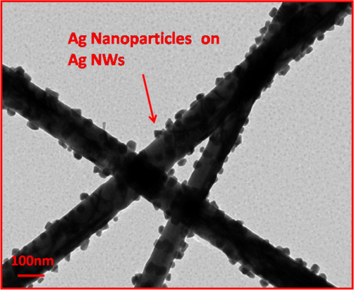
AgNWs irradiated by gamma rays of dose 12 kGy.
With the further increase in dose of γ-radiations up to 15 kGy, the diameters of NWs have also been reduced and AgNPs were appeared greater in number. TEM image of AgNWs irradiated by 15 kGy is shown in Fig. 8(a). Fig. 8(b) shows the SAED pattern of AgNWs irradiated by γ-radiations of dose 15 kGy. SAED pattern shows that structure of AgNWs is polycrystalline after γ-irradiations. So, γ-radiations of AgNWs lead to accelerate the formation of NPs on surfaces of AgNWs on the expense of diameters of AgNWs.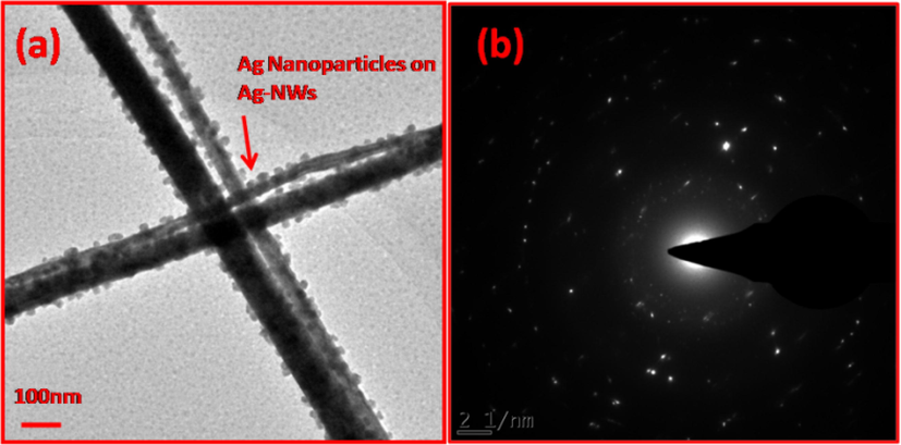
(a) TEM image of AgNWs irradiated by γ-radiations of dose 15 kGy (b) SAED pattern of AgNWs irradiated by γ-radiations of dose 15 kGy.
The optical characteristics of AgNWs containing AgNPs on outer surfaces are due to the surface plasmonic resonance and differ from the bulk silver material. Fig. 9(a–d) shows optical transmittance spectra of AgNWs containing AgNPs. As can be seen in Fig. 8(a–d), the spectra shows a low transmission and a strong absorption band of approximately 374 nm this is in ultraviolet (UV) region and may be due to the effect of surface plasmonic resonance (Pallavi Rana, 2014; Honey et al., 2016; Ziegler et al., 1985; Kumar et al., 2014). The absorbance band will appear in ultraviolet–visible (UV–VIS) spectra of AgNWs if the reduced wire sizes become up to nano-scale, however this band is not present in bulk silver (Kumar et al., 2014). This absorption band may be visible due to the interaction of the electron with the magnetic field. In fact, the interaction of electromagnetic field with AgNWs produces an oscillatory electric field and this moving or oscillatory electric field vibrates conduction electrons and the produce the displacement effect of electrons clouds associated with nuclei of material. The electron cloud moves around in relation to the nuclei due to the columb’s attractive force between the electrons and the nuclei (Kumar et al., 2014). The accumulated oscillations of conduction electrons are called surface plasmonic resonance (Kumar et al., 2014). This resonance is responsible for reducing transmission, enhanced dispersion and light absorption in UV environment. In the case of MNWs, these surface plasmonic bands lead to changeable and manageable optical properties of materials that can be used in a variety of applications. Additionally, it can be seen from Fig. 9 that transmittance (%) of current sample was increased initially with the initial doses of γ-radiations which increased significantly up to 90% with an increase in dose of γ-radiations up to 15 kGy. Subsequently transmittance was reduced by an additional incremental in dose up to 20 kGy which may be due to a factor created by the impact of the cascade collision. With the initial doses of gamma rays transmission may be enhanced due to the evolving of NPs on the outer surfaces of AgNWs.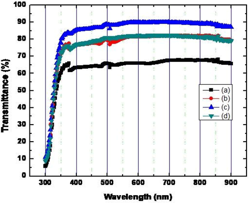
Transmittance spectra of AgNWs (a) un-irradiated (b) irradiated with γ-radiations of dose 12 kGy (c) irradiated with γ-radiations of dose 15 kGy (d) irradiated with γ-radiations of dose 20 kGy.
4 Conclusions
In summary, we obtained AgNPs on outer surfaces of AgNWs and also found high optical transmittance after γ-irradiation. We obtained most favorable results at doses 12 kGy and 15 kGy of γ-radiations whereas the results were not found to be optimal at 20 kGy. It is concluded that 15 kGy is probably the most favorable dose for γ-irradiation of AgNWs. From XRD results, it was clear that structure of NWs remains stable and does not change during γ-irradiation of NWs. Grain size was obtained from XRD data and it was first increased up to dose 15 kGy and later decreased at 20 kGy which might be due to production of defects in AgNWs after γ-irradiation at 20 kGy. Moreover, the values of strain and dislocation densities are firstly decreased up to dose 15 kGy which is might be due to improvement in crystalline quality of films and then increased at last dose 20 kGy which is might be due to production of defects. It was clear from TEM results that after irradiating AgNWs by dose 12 kGy of γ-radiations, AgNPs are formed on outer surfaces of AgNWs which are increased in number at 15 kGy on the expense of diameters of NWs which is reducing at this dose. From optical results, it is found that optical transmittance was increased after irradiation which is due to formation of NPs on Ag-NWs. This enhancement of optical transmittance is strongly related with growth of NPs. These NPs are formed due to accumulation of atoms which were ejected due to sputtering induced collision cascade of atoms. At high dose 20 kGy, transmittance has been reduced which is might be due to excessive initiation of sputtering, collision cascade and ejection of atoms which are producing more defects in the lattices. Therefore, the NPs deposition on surfaces of AgNWs is found to be excellent technique to enhance transmittance of AgNWs which is required for application of AgNWs as TEs in optoelectronic devices.
Acknowledgements
This research program was generously supported by grants from the National Research Foundation of South Africa (NRF), the French Centre National pour la Recherche Scientifique, iThemba-LABS, the UNESCO-UNISA Africa Chair in Nanosciences & Nanotechnology, the Third World Academy of Science (TWAS), Organization of Women in Science for the Developing World (OWSDW) and the Abdus Salam ICTP via the Nanosciences African Network (NANOAFNET) as well as the Higher Education Commission (HEC) of Pakistan to whom we are grateful.
Declaration of Competing Interest
The authors declare that they have no known competing financial interests or personal relationships that could have appeared to influence the work reported in this paper.
References
- Nano Lett.. 2010;10:2944.
- Nano Res.. 2012;5:805.
- Nat. Photon.. 2012;6:809.
- Groep J V, Spinelli P and Polman A 2012 Nano Lett. 3138.
- Org. Electron.. 2011;12:875.
- Adv. Mater.. 2011;23:1482.
- Chin. Phys. B. 2016;25:046105
- Mater. Res. Exp.. 2017;4:075042
- MRS Bull.. 2011;36:760.
- ACS Appl. Mater. Interfaces. 2013;5:788.
- Adv. Mater.. 2011;23:2469.
- Curr. Appl. Phys.. 2014;14:1547.
- ACS Nano. 2010;4:11.
- Nano Lett.. 2010;10:1276.
- Adv. Mater.. 2011;23:4371.
- Nanoscale Res. Lett.. 2011;6:75.
- Nanotechnology. 2010;21:215707
- J. Alloys Compds.. 2015;647:145.
- J. Materiomics. 2021;7:612.
- Pallavi Rana, R. P. Chauhan 2014 Physica B 451 26.
- Small. 2011;7:2621.
- Adv. Mater.. 2009;21:3210.
- J F Ziegler, J P Biersack and Littmark U 1985 Perganom Press, New York.