

Translate this page into:
Effects of gamma irradiation on the properties of Ce2S3 thin films
⁎Corresponding author. sdawood@ksu.edu.sa (S. Aldawood)
-
Received: ,
Accepted: ,
This article was originally published by Elsevier and was migrated to Scientific Scholar after the change of Publisher.
Abstract
Cerium sulphide (Ce2S3) thin films were prepared via successive ionic layer adsorption and reaction (SILAR) scheme. The optical, structural, and electrical investigations of both virgin and gamma-exposure samples were conducted, focussing on the gamma irradiation dose. The objective was to examine the impact of gamma irradiation on the characteristics of the Ce2S3 thin films. An X-ray diffraction (XRD) study of the samples established the orthorhombic phase of the Ce2S3 thin films and revealed that the crystallinity was improved with the gamma dose. The Field emission scanning electron microscope (FESEM) images of the virgin thin film detected a smooth surface with spherical grains with distinct grain boundaries. In contrast, after the gamma exposure, the thin film surface revealed a cluster of small particles. Energy dispersive X-ray (EDX) study inveterate the stoichiometry of the prepared Ce2S3 thin films. The gamma exposure dose caused a deviation in the bandgap, which was related to the quantum confinement effect. Photoluminescence (PL) spectra proved that the emission intensity of the Ce2S3 thin films decreased with increasing gamma dosage, and this phenomenon was attributed to the additional crystallites and a smaller number of structural defects. This simple approach to amend the characteristics of Ce2S3 thin films by gamma exposure could become an attractive option to explore this material for dosimetry and radiation sensing.
Keywords
Gamma exposure
SILAR
Photoluminescence
Energy band gap
Impedance spectroscopy

1 Introduction
Cerium is an earth-abundant material in the lanthanide series and is also designated as a rare-earth element. Rare-earth materials have exceptional metal colour pigments and distinctive luminescence characteristics [Kariper, 2014; Maqbool et al., 2007]. Additionally, sulphide chalcogenides have attracted considerable attention because of their arrangement of sulphur with metals. Owing to the multiple oxidation states of sulphur, this arrangement is likely to endow remarkable properties [Hui et al., 2021]. Cerium sulphide (Ce2S3) is an interesting material owing to its remarkable electrical and mechanical properties, such as thermal stability, electrical conductivity, and optical characteristics [Forster and White (2006)]. Cerium sulphides are mostly recognised as dicerium trisulphide (Ce2S3), tricerium tetrasulphide (Ce3S4) and cerium monosulphide (CeS) [Krikorian and Curtis (1998); Othmer (2010)]. They present three types of structural phases, namely orthorhombic alpha-Ce2S3, metabolic beta-Ce2S3 and hexagonal gamma-Ce2S3 by diverse structural, optical and electrical properties [Babonas et al., 1991].
Herein, we deposited an easy and simplistic in preparation method via a SILAR technique to deposited novel two-dimensional (3D) Ce2S3 thin film. The compensations of the SILAR technique, containing a large scale preparation, could be deposited on any substrate at room temperature and pressure by using simple practices and cheap tools [Agustin et al., 2022]. The composition, width, morphology, and grain size can be controlled [Jose et al., 2021].
Analyses of the effects of high-energy electromagnetic exposure on nanoscale semiconductor thin films is crucial for the development of radiation absorber for sensing and detecting ionisation radiation. Electronic applications demand materials that are capable of radiation-imposed scission or cross-connections, while aeronautics and medical applications require remarkably radiation-stable and radiation-absorbing materials [Rani et al., 2013]. Gamma irradiation can alter the nanostructure and charge carrier defect density in a semiconducting host, which transforms the irradiated materials via a measurable method [Arshak et al., 2008]. This modification depends on the radiation dose and susceptibility of the materials to precise radiation [Siedle and Adams, (1993)]. Nanoscale materials are broadly amenable to the use of biosensors because of their large surface area and excellent biocompatibility [Liu et al., 2003].
Several studies have examined the interaction of gamma rays with nanomaterials such as SnO [Abhirami et al., 2013], TeOx [Baydogan et al., 2013], InP [El-Nahass et al., 2009], and CoPc [Dewan et al., 2008]. Chalcogenide semiconductor nanomaterials have received increasing attention over the last few decades because of their extensive properties, such as high refractive index, wide IR transmission windows, chemical constancy, and the opportunity to alter their physical characteristics [Rajapure et al., 1997]. Recently, the effect of high-energy gamma irradiation on thin films of chalcogenide semiconductor materials, such as Se70S30−xSbx [Mitezsch and Fitzgerald (2000)], CuInSe2 [Ramaiah et al., 2000], Se1−xTex [Ibrahim and Soliman (1998)], and InSe [El-Nahass et al., 2013], has been investigated. The influence of gamma exposure on the physical properties of CuPbI3/Si heterojunction in the range high energy photon. This investigation has been approved to examine the appropriateness of the CuPbI3/Si heterojunction for the gamma dosimetry [Aldawood et al., 2023]. Irradiating thin films with high-ionisation-energy radiation generates structural imperfections or lattice defects in the form of deficiencies, as well as defect clusters owing to the heat transformation and dislocation atoms near the interface. Several other studies have examined the effects of gamma-ray irradiation on the physical characteristics of thin films [Aldawood et al., 2021; Ali et al., 2020; Ali et al.,2019; Ali, 2017].
In this study, the deposition, characterisation, and analysis of gamma-induced modifications in the structural, optical and electrical features of SILAR deposited Ce2S3 thin films were systematically investigated. The main motivation of this research was to assess the degree of radiation-induced alteration of the prepared Ce2S3 thin films, and promote the use of this material for radiation sensing and dosimetry applications. To this end, the nanostructural, electrical, morphological, and optical characteristics of Ce2S3 were experimentally measured at different gamma doses.
2 Material and methods
2.1 Chemicals
Ce(NO3)2 (Sigma Aldrich, 99.99 %) and Na2S (Sigma Aldrich, 99.99 %), were used.
2.2 Deposition of Ce2S3 thin films
The required Ce2S3 thin films were synthesised on glass substrates by means of the SILAR method. The concentration of ionic solutions, the pH values of the solutions, and the dipping and washing times were optimised to deposit uniform Ce2S3 thin films on the substrates. For the fabrication of the Ce2S3 thin films, a 0.025 M caesium nitrate Ce(NO3)2 cationic solution (pH∼8) and a 0.025 M sodium sulphide (Na2S) anionic solution (pH∼11) were used. In the first step, a washed glass substrate was immersed in the Ce(NO3)2 solution for 2 min to allow it to adsorb cerium ions onto the substrate, and then washed with deionized water (DIW) for 30 s to eliminate unattached ions and impurities. In the second step, the same substrate was dipped in the Na2S solution for 2 min to allow it to react with the sulphide ions and adsorbed cerium ions, and then washed with deionised water for 30 s. After the completion of these two steps, a SILAR cycle of the Ce2S3 thin film was accomplished. To obtain thin films of appropriate thickness, 35 SILAR cycles were repeated.
2.3 Thin film irradiation
The as-prepared Ce2S3 thin films were exposed to a gamma source Co-60 (Nordion, model GC-220) with a half-life of 5.27 years and exposure rate of 927.299 Gy/h. Three thin films of Ce2S3 were exposed to radiation doses of 250, 500, and 1000 Gy with varying exposure times.
2.4 Characterisation
The properties of the virgin sample and gamma-exposed Ce2S3 samples were observed with XRD (Panalytical X’Pert3) having a Cu-Kα of wavelength of 1.5406 Å as the X-ray source for the structural investigation. A morphological study was conducted using FESEM (FESEM; JEOL). The thicknesses of the thin films were measured using gravimetric analysis. Optical studies were performed using the transmission and photoluminescence spectra of the samples obtained via a UV–Vis spectrophotometer (JASCO V-670) and spectrofluorometer (JASCO FP-8200). An impedance analysis was performed using an impedance analyser (Hioki).
3 Results and discussion
XRD patterns of the virgin and gamma-exposed Ce2S3 films with different gamma dose exposures (250, 500, and 1000 Gy) are depicted in Fig. 1. The as-deposited Ce2S3 thin film crystallised into an orthorhombic phase structure (1 1 1) with a major diffraction located at a 2θ of approximately 25.45° (JCPDS-21–0189). It was observed that the predominant diffraction was narrow for the pristine sample, while the gamma-exposed thin films presented a decent crystallinity. The intensity of main peak increased considerably in the pristine sample. The decrease in the intensity of the peaks in the latter may be owing to imperfections or disorders generated after the gamma irradiation. The gamma radiation is expected to produce prominent structural deficiencies, thus reducing the peak intensity. Comparable results were previously reported for CoPc thin films [El-Nahass et al., 2013]. Most studies [Lehman, 1977] revealed physical changes, such as pair production photoelectric emission/absorption, Compton scattering, and pair annihilation when gamma rays interacted with nanomaterials. Furthermore, these irradiation phenomena are determined by the various dose and the structure of the host materials. During irradiation, the knocking of host atoms generates an appropriate amount of heat, that mains to the relocation of atoms by subordinate interactions, and creates numerous defects [Lehman, 1977]. Moreover, a slight broadening of the main XRD peak of the irradiated samples was also observed. These results agree well with those reported by Aldawood et al. [Aldawood et al., 2020].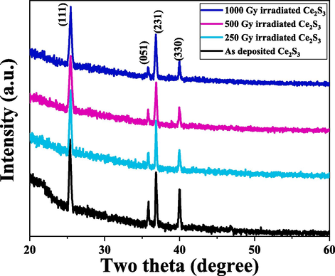
(a) XRD patterns of the virgin and gamma-exposed Ce2S3 thin films.
The nano-structural properties of the Ce2S3 thin films pre- and post-gamma irradiation with variations in gamma ray dosing value were computed by (1 1 1) orientation using the Debye–Scherrer formula (Eq. (1)) [Zinzuvadiya et al., 2019],
The crystallite size decreased with growing gamma irradiation dose, as shown in Table 1. This could be owing to the penetration of deep gamma rays into Ce2S3, thus causing alterations to the host thin film by pushing the basis from its regular lattice, and consequently breaking up the molecules into smaller particles. In this phenomenon, the gamma photons lose energy, which might generate or heal the defects in the structure [Raneesh et al., 2013]. This distortion in the crystal structure by gamma irradiation can be ascribed to each the deviation in the lattice deficiencies in the host materials or the decline of micro-strain in the gamma-exposed samples; this is also evident in the peak broadening [Dogra et al., 2003].
Gamma dose
(Gy)
Lattice Constants
(Å)
Crystallite size
(nm)
Micro-strain
(x10–3)
‘a’
‘b’
‘c’
0
7. 6596
15.9838
4.2863
84.38
18.62
250
7. 6734
15.9637
4.2863
73.67
21.15
500
7.6388
15.9883
4.2863
57.54
29.68
1000
7.6835
15.9729
4.2863
53.36
35.75
The lattice parameters of the Ce2S3 thin films in the orthorhombic phase were estimated from the XRD diffraction planes using the following equation:
FESEM was used to explore the effect of the gamma ray exposure dose on the morphological and surface properties of the Ce2S3 thin films. Fig. 2(a)–(d) illustrates the FESEM microphotographs of the as-prepared sample (0 Gy) and gamma-ray-exposed samples (250, 500, and 1000 Gy), respectively. As revealed in Fig. 2(a), the as-prepared thin film presented smooth and indistinct grain boundaries with a regular arrangement. Apparently, the sample exposed to a low gamma-ray dose (Fig. 2(b)) revealed that the irradiation did not propagate homogeneously and the film surface contained a mixture of small and clustered particles. However, at an exposure dose of 500 Gy, it can be seen from Fig. 2(c) that the small grains agglomerated, and clusters were enhanced compared to the sample irradiated with 250 Gy. At a high gamma-ray dose exposure (1000 Gy), as shown in Fig. 2(d), the surface of the thin film was clearly degraded, suggesting that high-energy transformation gamma-irradiated photons damaged the surface of the thin film. Additionally, more voids and gaps were detected, and the particle size decreased from 105 nm (in the pristine film) to 30 nm as the gamma ray dose was increased. The EDX analysis of the deposited Ce2S3 thin films is presented in Fig. 2 (e). The Ce and S configurations are accessible in Fig. 2 (e); this illustrates the purity of the Ce2S3 thin films.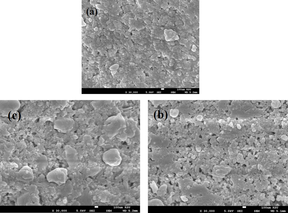
FESEM images of (a) virgin, (b) 250 (c) 500 and (d) 1000 Gy irradiated films; (e) EDX analysis of as-prepared Ce2S3 thin film.
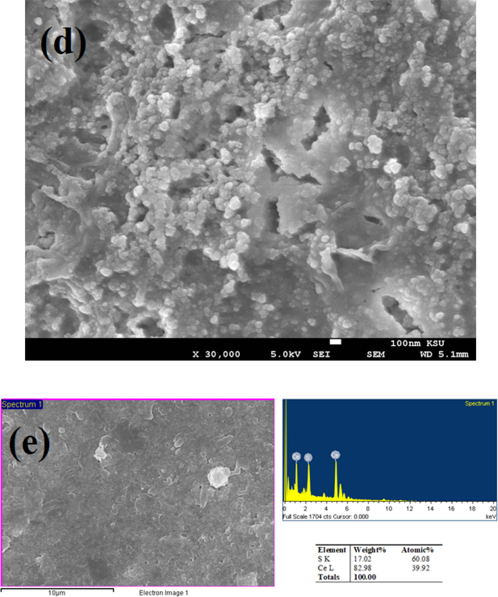
FESEM images of (a) virgin, (b) 250 (c) 500 and (d) 1000 Gy irradiated films; (e) EDX analysis of as-prepared Ce2S3 thin film.
The transmission spectra of the Ce2S3 thin films exposed to numerous gamma doses are shown in Fig. 3. As can be seen, the transmission decreased with the gamma dose value in the transparent region from 500 to 1050 nm, which indicates a decrease in the film’s transparency. This decrease in the transmission can be caused by large-scale scattering effects and structural inhomogeneity caused by the irradiation [Prathap et al., 2006]. It can be observed in the FESEM and XRD images that the grain size and crystallinity, respectively decreased after the gamma exposure. Thus, the lower crystallinity and linkage of grains increased the carrier diffusion, which in turn, enhanced the scattering effect [Gulen et al., 2013]. In the wavelength region near 700 nm, a redshift in the band edge was observed with increasing gamma dose, suggesting a corresponding decrease in the optical bandgap.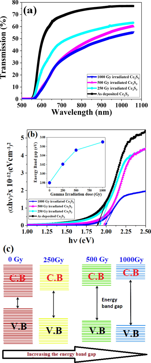
(a) Transmittance spectra and (b) Tauc’s plot for band gap calculation of the Ce2S3 thin films for different gamma irradiation doses; (inset) variation of band gap (c) Schematic diagram show the increase in the energy band gap with gamma irradiation of Ce2S3 thin films.
The band gap (Eg) is an important factor in various advanced applications of nano-scale. To compute the band gaps of the Ce2S3 thin films UV–Visible transmission spectra were used. To analyse Eg, the optical absorption coefficient (α) values were obtained using Equations (4) and (5):
From Fig. 3(b) it can be observed that the energy band gap surges upwards after the exposure. The inset of Fig. 3 (b) presents the optical energy band gap of the pristine thin film as well as gamma-irradiated thin films before and after the irradiation. Generally, the energy band gap increased with gamma irradiation because of the upsurge of electron owing to a rise in the Fermi level in the conduction band [Ejderha et al., 2010]. Prathap et al. [Prathap et al., 2006] described this effect of gamma irradiation on the gradation of crystallinity of the thin films. After the gamma exposure, the trap concentration in the conduction and valence bands of the thin films would be dependent on the irradiation dose level. Thus, by effectively controlling the gamma radiation doses, the electronic properties of the interacting thin films could be meaningfully altered [Aldawood et al., 2022]. Aldawood et al. described similar phenomena in gamma-exposed PbI thin films [Aldawood et al., 2022].
On the basis of the above results, the schematic diagram of the band structures of the Ce2S3 thin films before and after the gamma irradiation are revealed in Fig. 3 (c). After gamma irradiation treatment, energy band gap increased with the gamma dose value.
The PL spectra of the as-prepared and gamma-exposed Ce2S3 thin films were obtained at an excitation wavelength of 615 nm to evaluate their structural quality, photoluminescence properties, and defects. The room-temperature PL spectra of the as-prepared and gamma-irradiated samples with different gamma doses are shown in Fig. 4. One broad PL peak was observed at 652 nm (1.9 eV) in both the as-deposited and irradiated thin films; this was associated with the luminescence emission caused by the transfer of electrons from the valence band to the conduction band. The observed luminescence emission was in good agreement with the band gap of the Ce2S3 thin films measured using UV–vis spectroscopy. The shift in the main peak toward a shorter wavelength with increasing gamma irradiation dose could be owing to the increase in the optical band gap energy and the increase in the intensity, caused by an additional amount of carriers transferred from the valence band to the conduction band. In addition, a slight hump was observed near 648 nm at 250 Gy, which was attributed to the emission associated with Ce vacancies on the in the Ce2S3. The conversion from a slight hump to a sharp defect peak and the decrease in the intensity with increasing gamma irradiation dose could be due to the variation in the surface defect density or a lower recombination rate. The observed changes in the defect peaks indicate an structure improvement in the of the Ce2S3 with increasing the gamma dose [Memesa et al., 2011].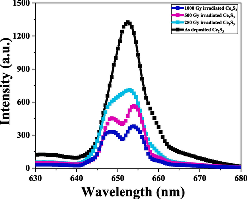
PL spectra of the Ce2S3 thin film for different gamma doses.
Electrical impedance spectroscopy was conducted to understand the mechanism of charge transformation through the Ce2S3 thin films and effects of gamma irradiation on their electrical properties. Typical Nyquist plots of the thin films at different gamma irradiation doses are shown in Fig. 5. The experimental data were obtained using ZView software, and the equivalent circuit model was used, as illustrated in the inset of Fig. 5. The suggested equivalent circuit included the grain resistance (Rg), grain boundary resistance (Rgb), and grain boundary capacitance (Cgb). The simulated curves (solid lines) agree well with the experimental results (symbols), suggesting that the preferred circuit model is feasible. The computed values of the equivalent circuit components are listed in Table 2.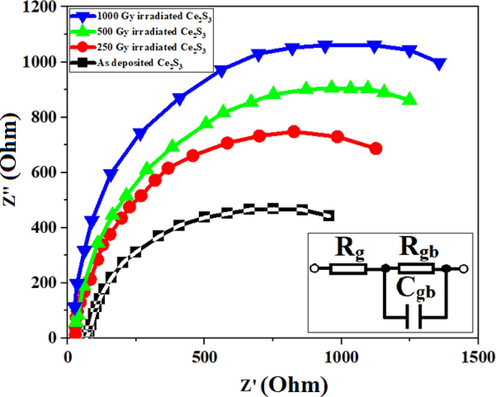
Nyquist plots for various gamma doses; (inset) proposed equivalent circuit of the model.
Gamma exposure dose (Gy)
Rg (Ω)
Rgb (kΩ)
Cgb (pF)
0
86.93
1469.26
89.63
250
68.44
1684.73
88.97
500
59.71
2526.47
90.22
1000
54.34
2821.52
88.71
The irradiated Ce2S3 thin films exhibited greater resistance than the as-deposited thin film; this resistance increased with the gamma dose. This behaviour could be ascribed to a reduction in the carrier concentration when the Ce2S3 thin films were irradiated with gamma rays, which in turn, resulted in an increase in the electrical resistance. This could also be attributed to the agglomeration of crystallites at the grain boundaries, which produced defect states, and the consequent increase in the total resistance.
4 Conclusion
Thin films of Ce2S3 were deposited using successive ionic layer adsorption and reaction (SILAR) technique. The influence of gamma exposure on the structural, optical, and electronic characteristics of the deposited thin films was examined. The XRD patterns revealed that the crystallite size of the Ce2S3 thin films reduced from 84.38 to 53.36 nm upon increasing the gamma dose. The energy band gaps of the as-deposited and gamma-irradiated thin films were measured using UV–vis transmission spectroscopy. The optical band gap decreased slightly from 1.88 to 1.99 eV as the gamma dose increased. On the other hand, the PL intensity of the broad peak decreased with increasing gamma dose, which was manifested as an enhancement in the crystallinity and reduction in the defects in the gamma exposed thin films. Impedance analysis shown that the irradiated Ce2S3 thin films offered larger resistance than the as-prepared thin film; furthermore, this resistance raised with the gamma dose.
Research involving human and/or animal participants.
This article does not contain any study conducted by any of the authors involving animals and human participants.
Acknowledgements
The authors extend their sincere appreciation to the Researcher Supporting Programme at King Saud University, Riyadh, for funding this work under Project Number: RSP2023R328.
Declaration of competing interest
The authors declare that they have no known competing financial interests or personal relationships that could have appeared to influence the work reported in this paper.
References
- Radiat. Phys. Chem.. 2013;91:35-39.
- Processes.. 2022;10:492.
- J. of King Saud University – Sci.. 2020;32:2629-2634.
- J. Mater. Res. Technol.. 2021;14:108-120.
- Radi. Phy. and Chem.. 2022;193:110003
- Mater. Chem. Phys.. 2023;309:128420
- J. Mater. Sci: Mater. Electron.. 2017;28:16314.
- Mat. Sci Semi. Proc.. 2019;93:44-49.
- Radiat. Phys. Chem.. 2020;171:108732
- Thin Solid Films.. 2008;516:1493-1498.
- Phys. Coll.. 1991;31:73.
- Radiat. Phys. Chem.. 2013;89:20-27.
- Sens. Actuat.. 2008;147:115-120.
- Nucl. Instrum. Method B.. 2003;207:296.
- Superlattice Microstr.. 2010;47:241.
- Appl. Surf. Sci.. 2009;255:9439-9443.
- J. Non-Cryst. Solids.. 2013;382:74-78.
- Mater. Res. Bull.. 2006;41:448.
- Mater. Electron.. 2013;24:467-474.
- Carbon Energy.. 2021;3:709-720.
- Radiat. Phys. Chem.. 1998;53:469-475.
- Processes.. 2021;9:967.
- Prog. Nat. Sci. Mater. Int.. 2014;24:663-670.
- High Temp. High Press.. 1998;20:9-18.
- Interaction of Radiation with Solids and Elementary Defect Production. North-Holland Publishing Company; 1977.
- J. Electroanal. Chem.. 2003;540:61.
- Appl. Phys. Lett.. 2007;91:193511
- Colloid Polym. Sci.. 2011;289:943.
- J. Appl. Surf. Sci.. 2000;16:162-163.
- John Wiley & Sons USA.. 2010;5(2010):670-677.
- Mater. Chem. Phys.. 2006;100:375-379.
- Thin Solid Films.. 1997;311:114-118.
- Mater. Lett.. 2000;45:251-261.
- Radiat. Phys. Chem.. 2013;89:28-32.
- Handbook of Radiation Effects. Oxford, New York: Oxford University Press; 1993.
- J. Magn. Magn. Mater.. 2002;250:77-82.
- Thin Solid Films.. 2019;669:525-530.